Six degrees of preparation: The six life stages of every product

The-six-life-stages-of-every-product

Every product we own, desire or leave on the shelf has its own story. From being a mere twinkle in its designer’s eye to the sad day when its parts are being recycled for newer, more exciting models, there is always a myriad of processes and considerations that go into creating that product.

But what’s actually involved in making a product?

Here’s our step-by-step guide to the six stages involved in every product’s lifecycle, from concept to obsolescence and how choosing the right manufacturing partner can make these steps easier to manage.

1. Design: Defining the idea

Design
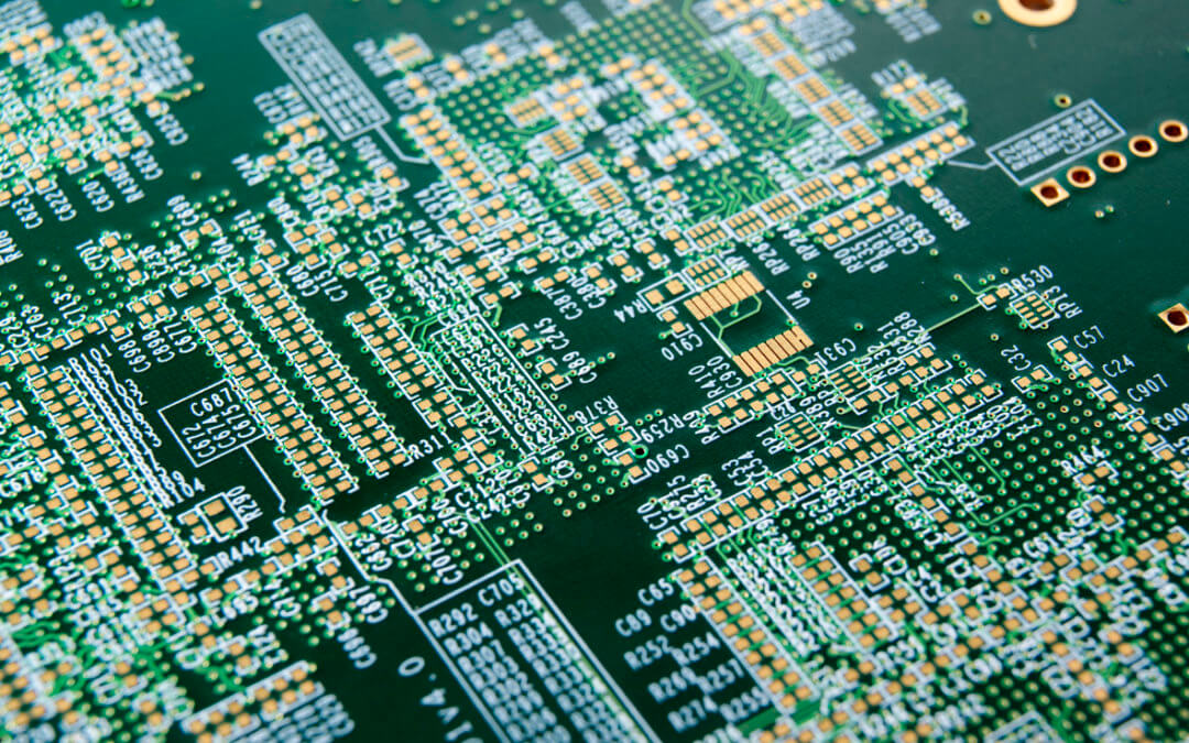
Designing a product is never simple.  When that product contains complex electronic circuits and components, the design process is even more complicated, needing to take into account the following considerations:

  •  Component selection. It is easy to default to known, and previously used, families of parts but the market is volatile and subject to change. It’s vital to determine whether selections are truly optimal for sustainable supply across the entire product lifecycle.
  • Which materials can withstand the conditions the product will be used in, for example hostile, hazardous or security sensitive environments.
  • The design will meet functionality requirements, but is the construction design effective and facilitate use of the latest manufacturing automation?
  • How the product can deliver both optimal function AND cost-efficiency

Using a manufacturing partner skilled in Design for Manufacture (DfM) will help to ensure that whatever solution is chosen will be cost-effective and adhere to the Bill of Materials (BoM)

However, it’s also important to incorporate processes that will enable a smooth manufacturing operation. Influencing the design while it is still fluid is crucial so difficult and costly decisions don’t need to be taken later in the process.

An EMS partner can work with customer teams to devise design packages and create documentation such as Gerber data, or take developed packages and get them ready for the the later stages of manufacturing.

Whatever stage they become involved at, the NPI engineers’ priority will be to take a customer’s concept and turn it into a tangible plan for volume manufacture.

2. New Product Introduction (NPI): Turning plans into process

NPINPI is arguably not a single step on its own, but rather an enabler for the rest of the manufacturing process, but it deserves the number 2 spot in this list as what comes next in the product lifecycle cannot be achieved without it.

It is at the NPI stage that the ideas that were developed and shaped during the design stage can be turned into workable processes. The initial plans are transformed into the building blocks for the manufacture itself, paving the way for the physical build of the product.

As supply chains get tighter, processes get stricter and timescales get shorter, global manufacturers are competing to satisfy the requirements of savvier, more demanding consumers.

Meeting these challenges head on is crucial to the NPI process, which demands a smooth transition from the design phase, into manufacturing and finally out to market.

The NPI engineering team will collaborate with customers on any aspect of data translation, documentation, design, assembly and test to create an optimal package, with stages formally validated at each gate.

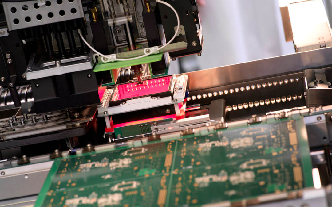
3. Rapid Prototyping: Enabling a smooth transition to manufacture

Rapid prototypingEvery new electronic product needs to be tried and tested before being launched to market. Rapid prototyping is the quickest and most seamless way to reduce the speed to ramp, while maintaining product quality and lowering costs.

Product and circuitry tests conducted early in the manufacturing journey are not only better for our customers, but mean that products can be modified quicker and out to market faster.

Software development is often delayed until a working hardware platform becomes available, so the prototypes are needed beforehand.

Rapid prototyping doesn’t just benefit customers who need a working version of their product to validate that the circuits function perfectly; it also shows design teams that the circuits fit into the size and space required, which then can be vigorously tested and qualified to meet regulatory requirements.

It’s best to use the same equipment for prototyping that you will use for volume production, so you can check the product’s readiness for large scale manufacturing and pave the way for a smooth transition.

4. Supply Chain Management: Establishing sustainable sourcing procedures

Supply chain managementSetting up a supply chain that will guarantee on-time delivery, cost savings and sustainability of components is crucial when preparing any product for a smooth route to market.

Once prototypes have been approved and testing is complete, establishing the correct sourcing solutions is a vital step in the product lifecycle. From choosing the best suppliers for each component to auditing each supplier and testing their capabilities, it’s hugely important to make these preparations before volume manufacturing can begin.

EMS partners need to understand the following before they can start to establish the best sourcing options for each product and customer:

  • Product lifecycles
  • Timeframes
  • Urgency
  • Quantities required

Additionally, it’s important to know if products need to meet certain standards, for example, if they have to be built to military grades or other strict regulations. Market conditions and current component stocks will also affect where and when you begin your sourcing journey.

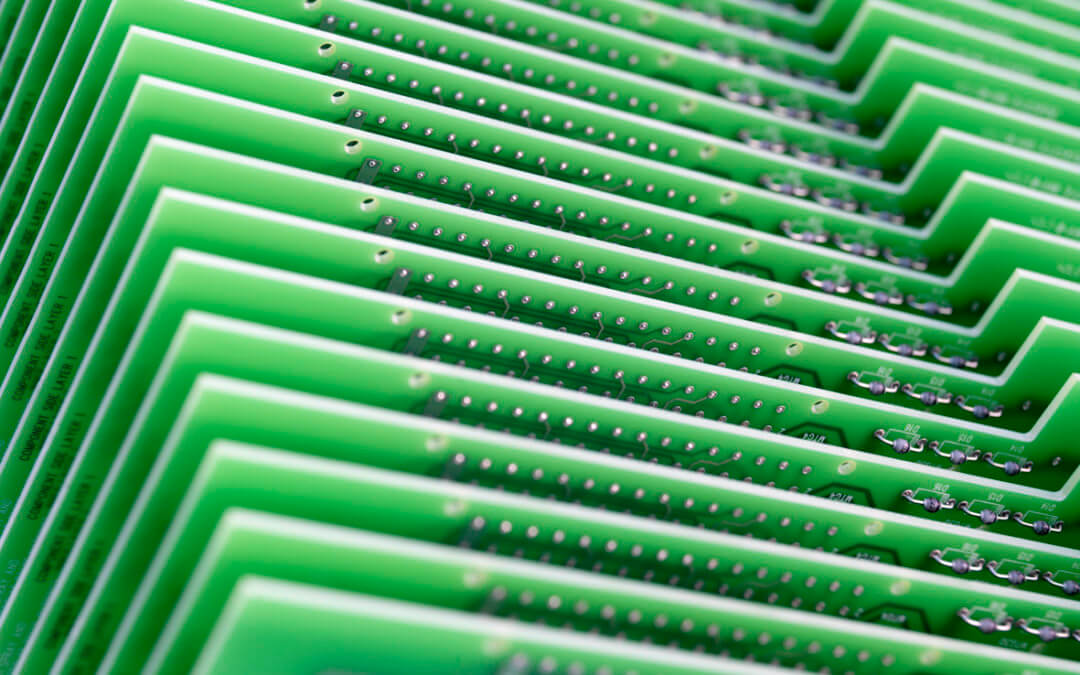
5. Volume manufacturing: Combining intelligent solutions with optimal process

Volume manufacturingThe ‘manufacturing’ part of the process only comes when the previous steps have been taken: managing the actual production lines and taking the product through to fulfilment and shipping is (almost) the final piece of the puzzle.

The ins and outs of the manufacturing process itself are countless, from specific techniques involved such as surface mount and through hole assembly and specialised services such as conformal coating and complex solderwork.

Each customer and each product requires a different combination of processes, techniques, testing and analysis throughout the manufacturing stage to ensure it is fit for the end-user.

Once sub-assembly build is complete, systems integration stages such as box build, electro-mechanical assembly, wiring, firmware programming/software upload, test, configuration and encapsulation can then take place to “create” an actual product.

Before shipping, comprehensive inspection and packaging is applied to ensure products are ready to be delivered to their ultimate destination.

6. Legacy products

Legacy ProductsManaging the end of life of a product is an essential part of the wider lifecycle support system that an EMS partner will provide its customers, from concept to the legacy stage.

Lifecycle support also includes crucial services such as returns management, repairs and warranty management, all of which can be undertaken or overseen by an EMS partner.

Managing a product decline can be tricky, as volumes start to reduce and materials become difficult to source, especially if the product is an older model using components which may now be bulky, outdated or simply hard to get hold of.

It’s not just the components either; older tooling and equipment may wear down over time and if fewer products require their use, it can be costly and ineffective to replace them.

Different solutions can be applied to end of life situations: some products get superseded by newer models or versions, meaning only slight tweaks to the manufacturing and sourcing procedures.

Other products may simply need support as they dwindle, which can involve investing in enough stock and parts to last the predicted period before they are withdrawn from the market.

It’s vital that all parties understand the market and technological dynamics that can lead to physical parts being renumbered following a change in supplier or manufacturer. Once again this requires in-depth knowledge and monitoring of the entire supply chain.

By working with a manufacturing partner which is dedicated to monitoring the market for signs of change and has the knowledge to react to this and find suitable alternative routes, this process can be managed effectively without compromising timescales or cost.

Four critical questions to ask your EMS provider about your data’s security

We live in a connected world.

The Internet of Things (IoT), the ubiquity of data and the Fourth Industrial Revolution deliver gains in productivity and efficiency through connections across the manufacturing sector.

Yet the same connections that strengthen us could also weaken us: as our shared data becomes more powerful it could prove to be our Achilles heel.

And it’s the weak link in the chain that hackers are increasingly keen to exploit.

The importance of security for electronic manufacturing

Recent concerns have highlighted how security threats could derail the application and uptake of IoT.

A study released by Hewlett-Packard discovered that 70% of the most commonly used IoT devices contain at least some vulnerabilities.

A review of these breaches led a contributor to New Electronics to bemoan that ‘vendors are repeatedly failing to apply simple security best practise and are exposing their customers to attack.’

The article goes on to list ten common security breaches, among which it includes issues with the hardware itself.

  • Unnecessary functions such as debug ports are left in place creating potential routes in for hackers.
  • Devices are under-utilising security mechanisms such as BGA (Ball Grid Array) packages which, when combined with good PCB design, make it harder to tap into signals.

But these concerns about security are not just about the end-products but can be found in the manufacturing process itself.

Here are some of the stories that have hit the headlines in the last few years:

  • Electronics manufacturer Foxconn was breached by a hacktivist group that released every employee’s login information.
  • Boeing was compromised repeatedly for four years by foreign nationalists trying to steal defence program manufacturing plans.
  • In Japan, Korea and Germany manufacturers have been targeted by hackers, believed to be from China, trying to access IP data, trade secrets and blueprints.

And here’s a story that did not make quite such a big splash but is even more alarming.

  • 48% of UK manufacturers have been subject to a cyber-attack – and half of these businesses suffered either financial loss or disruption to business as a result.
  • Manufacturing is now the third-most targeted sector for attacks by hackers.

These shocking statistics are from a report on cyber-security for manufacturers, published by EEF and AIG and carried out by the Royal United Services Institute (RUSI).

It goes on to suggest that this threat will only deepen with increasing digitisation – and notes that 91% of manufacturers are investing in digital technologies.

The report also found that across the manufacturing sector cyber security maturity levels are ‘highly varied’ both in terms of awareness of the cyber security challenge and the implementation of appropriate risk mitigation measures.

Which suggests there are many weak links in the supply chain out there.

Critical questions to ask your EMS provider

The good news for electronic manufacturers is that GDPR has helped to focus minds. Manufacturers are increasingly willing to question their suppliers to ensure adequate security procedures are in place.

The EFF/AIG report found that 58% of manufacturers have been asked to demonstrate or guarantee the robustness of their cyber-security processes by a business within their own supply chain.

Worryingly, 42% haven’t.

And of even more concern is that 37% of manufacturers admitted they would be unable to do this if asked today.

If you are looking for an EMS provider to partner with here are four critical questions you should ask about their security arrangements.

(We’ve provided our own answers after each one.)

1/ How do you ensure the security of your customer’s product data?

  • Our data is stored in a protected area that has restricted access.
  • Data is only ever distributed on a need to know basis.
  • Our network has strict access controls, with verification required at each level of security.
  • We do not outsource any area of your PCB assembly – to ensure there is no risk of compromise from this.
  • We manage our supply chain robustly, establishing long-term relationships and always ensuring Non-Disclosure Agreements are in place where needed.

2/ How do you ensure security on-site?

  • Our site has controlled access – this extends to each facility and internal area.
  • We carefully manage any contractors on site – access to customer data is never granted to anyone not employed by Chemigraphic.
  • The data itself is stored in a vault storage.
  • We have access-controlled IT server rooms.

3/ How do you manage your supply chain to ensure data security?

  • As the outsourced manufacturing partner to our customers, we take full responsibility for the entire manufacturing process and the management of any suppliers and materials within it.
  • We source excellent materials using only reputable partners.
  • We have enhanced inspection and qualification procedures for new parts to minimise the risk of counterfeit parts with security feature defects or malicious designs.
  • We undertake supplier site security audits if necessary – especially for overseas suppliers.
  • All employees and contractors are thoroughly screened.
  • If you prefer, we can work only from UK sources.
  • We discretely manage customer information, including the restriction of signage and non-publicity clauses etc.
  • We offer segregated materials storage and build areas – and we can provide a dedicated restricted-access area for security-conscious customers.

4/ Can you show me an example of a project of yours that had high security requirements?

Sure.

This case study of our work with a cyber-security sector customer is just one example of a project we’ve delivered where customer data and through processes were highly important.

Ask us about your data’s security with us

Everything we do is governed by robust processes. These are designed to meet exacting standards of security while delivering optimal efficiency and consistently excellent results.

We believe that through intelligent planning, proper process and strict control, anything can be achieved.

If you’d like to know more about how we ensure your data is safe and secure with us, don’t hesitate to ask or take a look at why we stand out from the crowd.

From art to science – the development of the PCB

From-art-to-science-1080x675

We recently outlined the evolution of the PCB after it emerged to replace point to point connections on a chassis in the years following World War II.

Here we’d like to trace the key moments in recent years that our brief history did not allow us space for.

As we chart how the manufacture of PCBs transformed from an art to a highly-specialised science we pinpoint five decisive moments that have kick-started their development in recent decades.

In the beginning

The earliest PCBs were very much works of art.

Etched by hand, they owed more to technology from artwork reproduction than to high tech.

To create these circuits copper-clad boards were used. The artwork was hand-drawn, and once the track layout was defined, it was printed onto the board as an etch-resist mask. Acid was next used to etch away the exposed copper before another chemical removed the etch resist.

Although we would still recognise the circuit board produced today, the process of producing it had its roots squarely in methods that had long been used in printing and artwork reproduction.

These processes have changed much since the tech breakthroughs and the manufacturing and electronic development that came to a head in the 1990s.

Here are just five of the ways that PCB manufacture was transformed from an art to a science.

The multilayer breakthrough thanks to via

It was in the 1990s that the use of multilayer surface boards became more frequent, allowing for greater complexity and speed.

The inevitable reduction in size of PCBs allowed them to be incorporated into a wider range of designs and devices.

What  the introduction of blind via and buried via permitted was connection on different layers through copper-plated holes functioning as an electrical tunnel through the insulating substrate. In the past connection through layers had been allowed using plated thru-barrels, but these created an obstacle to connections to every other layer.

The result, following the introduction of via technology in 1995, was the production of High-Density Interconnect (HDI) PCBs.

These could accommodate a much denser design on the PCB and allowed the use of significantly smaller components. With multilayer HDI PCBs reliability is enhanced in all conditions, which is why the most common applications for HDI technology are computer, mobile phone components, medical equipment and military communication devices.

Via have continued to evolve, with the recent emergence of micro-via, a specific type of small via which is used on particularly high-layer-count, densely populated PCBs, which are typically performing some form of high-speed number crunching.

Leadless components and the shrinking PCB

As we’ve seen PCBs really started to shrink in the 1990s (and they haven’t stopped since). Alongside the use of micro-vias we also saw the advent of leadless component designs, such as BGAs, uBGAs, chip-scale packages and so on.

These paved the way for integrated circuits with more gates which ushered in the start of successfully embedding memories and Systems on Chip (SoC) together.

Leadless packages save space by keeping the contact points in a matrix underneath the component instead of squeezed side-by-side around their perimeter. This extra space is crucial for applications like mobile devices, tablets and wearables, where every millimetre counts.

However, leadless packages also have a great deal of mechanical strength, so they don’t separate from PCBs as easily. This is thanks to their high contact area to package ratio which allows them to withstand a great deal of pulling and shear forces.

Since leadless devices are suspended on a matrix of underside solder spheres rather that soldered pins around the perimeter, manufacturing and inspection techniques need to be much more sophisticated, but the space-efficiency and reliability benefits are compelling.

Flexible circuits transform PCB designs

It was, again, in the 1990s that flexible circuits really made their presence felt, although their history can be traced all the way back to the birth of the PCB itself.

With the first PCB manufactured by Paul Eisler less than a decade old, we find a published exploration by Cledo Brunetti and Roger W. Curtis in 1947 of creating circuits on flexible insulating materials. Indeed, by the 1950s Victor Dahlgren and Royden Sanders had already made significant advances in actually developing processes that could print and etch flat conductors on flexible base materials.

Today, flexible circuits are produced by mounting electronic devices on flexible plastic substrates (such as polyimide, PEEK or transparent conductive polyester film) or by screen printing silver circuits on polyester.

They offer several advantages for many applications. These include their potential to replace multiple rigid boards, their suitability for dynamic and high-flex applications and their ability to be stacked in various configurations.

You will find them in:

  • Tightly assembled electronic packages, where electrical connections are required in three axes, such as cameras.
  • Electrical connections where the assembly is required to flex, such as folding mobile phones and laptop screen hinges.
  • Connections between sub-assemblies to replace the bulky and heavy wire harness, such as in cars, laptops, rockets and satellites.
  • Electrical connections where board thickness, weight or space constraints are important factors.

The finishes that created new beginnings for the PCB

The range of finishes that have been introduced into PCB manufacture over the last 20 years has also greatly enhanced their suitability for use in a number of applications.

The finish is applied to ensure solderability and to create the base of electronic connection between board and device. But, the correct surface finish selection can also affect PCB reliability – and the introduction of new finishes has greatly enhanced their reliability under a number of different conditions.

  • HASL

The traditional finish is Hot Air Solder Levelling (HASL) but this is now increasingly being replaced by lead-free HASL.

All HASL finishes prevent oxidation from the underlying copper but the process causes high stress on the PCB and this can diminish its long-term reliability. The process is also not suitable for HDI PCBs.

  • ENIG

ENIG (Electroless Nickel Immersion Gold) offers a great alternative – but one that comes with a price tag.

Ideal for fine pitch, flat surfaces, ENIG perfectly suits the modern-day HDI PCB. It can, however, carry undesirable magnetic properties and is prone to a build-up of phosphorous that may cause faulty connections and fractured surfaces.

  • OSP

OSP (Organic Solderability Preservative) is a finish that can be considered for fine pitches, BGA and small components. In addition, it is less expensive than ENIG and highly repairable, but it is difficult to test and has a limited shelf life of six months.

The rise of the exotic substrate

PCB manufacture has over the years gradually settled on the glass epoxy laminate of FR-4 as its preferred material.

There is good reason for this – in terms of performance and affordability – but we have, in recent times, seen the introduction of a number of alternatives. These ceramic and metallic substrates are often suited to specialist applications, such as those requiring performance in conditions of high temperature and high power.

They include:

  • Aluminium
    Used for parts requiring significant cooling, such as power switches and LEDs.
  • Kapton
    A polyimide foil used for flexible printed circuits that is resistant to high temperatures.
  • FR-5
    Woven fiberglass and epoxy offering high strength at higher temperatures.
  • G-10
    Woven glass and epoxy offering high insulation resistance, low moisture absorption and very high bond strength.
  • G-11
    Woven glass and epoxy offering high resistance to solvents as well as high flexural strength retention at high temperatures.
  • RF-35
    Fiberglass-reinforced ceramics-filled PTFE (Teflon) offering good mechanical and high-frequency properties.
  • Polyimide
    A high-temperature polymer offering excellent performance that can be used from cryogenic temperatures to over 260 °C.

The return of the art of the PCB

The diversity of today’s PCB technology requires an artist to create the perfect board for each device, application and customer.

Chemigraphic has the broad expertise and capability in each specialist area to understand and decide which technology and processes will create the right PCB for your requirements and budget.

Is the future of manufacturing additive?

The potential uses for 3D printing were widely misunderstood when it first appeared on the scene.

Tech pundits and futurologists joined forces to proclaim that 3D print would usher in a consumer revolution, as individuals took control of the means of production for themselves.

But, as we highlighted in our last blog, the benefits of 3D printing are now actually reshaping the manufacturing sector, rather than making it redundant.

The trend towards Additive Manufacturing

You can chart the change in the perceived benefits of 3D printing. As it changes from being seen as a consumer tool to a production tool, the use of the term ‘Additive Manufacturing’ (AM) dramatically rises.

This is how searches for AM are reported by Google Trends:

additive manufacturing

3D printing and AM are now used interchangeably as terms.

Peter Zelinski, the editor-in-chief of Additive Manufacturing magazine, reminds us we should bear in mind that AM also refers to other technologies and processes.

These include:

  • Rapid prototyping
  • Direct digital manufacturing
  • Layered manufacturing
  • Additive fabrication

Revealing synonyms

Synonyms, other than 3D printing, that are increasingly used for AM hint strongly at the benefits it offers – and that we will review further below:

  • Desktop manufacturing
    Suggests how AM frees production from the tyranny of tooling
  • Rapid manufacturing 
    Echoes rapid prototyping
    Suggests the speed of both prototyping and manufacture that 3D print offers
  • On-demand manufacturing
    Echoes on-demand printing
    Suggests the ability to cost-effectively create bespoke, tailored products


Additive Manufacturing

AM describes any technology that creates something by cumulatively adding layers of material.

The range of materials that can be used is ever-expanding and includes plastics, metals and concrete. In the very near future advances in biotechnology will inevitably see human tissue included in this list.

The basis of AM is computerised 3D modelling (or CAD). The data from this is used to add successive layers of liquid, powder or sheet material to manufacture a 3D object.

AM is fundamentally different to traditional manufacturing processes. These typically have a high up-front cost that is related to the need to create tooling.

  • Moulds are required by formative manufacturing technologies (such as injection moulding)
  • Cutting tools are needed for subtractive technologies (such as CNC machining).

The uses of Additive Manufacturing

This is what AM does well:

  • It is best suited to the production of single (or a limited number) of parts
  • It has an incredibly quick turnaround time
  • It has very low set-up costs
  • It can produce complex geometric shapes that are not producible using traditional manufacturing methods

In the past it was the case that the lower strength of objects it created could be an issue – and similarly it had proved wanting where functional parts with tight tolerances were called for – but this is increasingly not the case.

For instance in 2017, Siemens created the first gas turbine blades ever produced using 3D printing. Following performance testing under full-load conditions, these blades were found to survive temperatures above 1,250oC and pressures similar to the weight of a double-decker bus.

 Siemens created the first gas turbine blades ever produced using 3D printing

Source: Future Makers

What’s more, the blades traditionally took over a year to make but, with 3D technology, they took just eight weeks.

Early uses of AM harnessed its benefits for rapid prototyping, but more recently it is being used to fabricate end-use products in aircraft, dental restorations, medical implants, automobiles and even fashion products.

“This technology will impact pretty much every market sector, whether it’s shoes, whether its clothes, automobile parts, aeroplane parts, medical devices or electronics.”

Michael Todd, Global Head of Innovation at Henkel

Source: 3D metal work printing (image courtesy of Davidfotografie/Arup).

The benefits of Additive Manufacturing


The speed of production and lack of tooling requirements are a big plus for manufacturers. They enable designers to rapidly and cost-effectively prototype designs for verification and testing. In the past it took days or even weeks to receive a prototype – now AM places a model in the designer’s hands within hours.

This speed is further enhanced by the efficiencies AM can offer. Most parts require a large number of manufacturing steps to be produced traditionally, but AM completes the build in just one step. Freed from the constraints of, for example, machining and welding, new designs and possibilities can be explored.

For single (or low) volume runs, AM’s lack of tooling offers distinct cost advantages. It removes the need for a skilled machine operator to be present during the manufacture.

It is these cost and time benefits that have led to many innovative uses of AM. Nowhere is this more so than in the production of customised products. It is now possible to reduce the cost of bespoke products such as dental implants, hearing aids, prosthetics and, perhaps even in the near future, body tissue.

As well as medical and dental uses this capability is also seeing AM used for specialised military, automotive and aeronautical parts, as well as for customised fits on sporting equipment and fashionwear.

Is additive manufacturing the future?

As consumer trends move toward customisation, and increased competition demands lower and lower lead times, there is a clear place for AM in the future.

And it’s looking like it can disrupt niche manufacturers requiring specialist tolerances and precision as well as those serving the mass, consumer market.

At present, there are two main factors that restrict its use:

  • Scalability
    AM still can’t cost-effectively manufacture higher volumes of products
  • Versatility
    The range of materials that AM can use for manufacture is expanding but, for example, it still struggles to handle true silicones

However, its capabilities are continually expanding.

And it’s here to stay.

Richard Hague, Professor of Innovative Manufacturing at the University of Nottingham, firmly stakes its place in the future of manufacturing:

“I don’t think additive manufacturing is an emerging technology any more. I think it’s emerged, and many people are already using it – and using it successfully.”

How is 3D printing freeing up design space?

“If by some miracle some prophet could describe the future exactly as it was
going to take place, his predictions would sound so absurd, so far-fetched that everyone would laugh him to scorn.”
Arthur C. Clarke, author, speaking in 1964

Science fiction writer Arthur C. Clarke went on from making this observation to describe the forthcoming advent of 3D printing.

And, sure enough, it came to pass.

Today, as 3D printing quite literally breaks the design and manufacturing mould across a range of sectors, it’s time to assess its true impact and where it may take us next.

The path that 3D printing has taken bears very little resemblance to what the prophets foresaw. Throughout the early years of the new millennium, futurists prophesised it would usher in a new consumer society. In this brave new world, the need to visit shops to buy things would be gone – and so too would the need to rely on online retailers’ massive warehouses to deliver our goods.

Soon, we were told, we would all be downloading a design file to our personal 3D printer and manufacturing our products – exactly as we wanted them to be – from the comfort of our homes.

Of course, this consumer revolution never happened.

However, a sea-change is quietly washing over the design, manufacturing and production sectors, one that is not deluded tech fantasy, but very real indeed.

Richard Hague, professor of innovative manufacturing at the University of Nottingham, compares the hype and reality of 3D printing with the dotcom crash of the late 90s.

“There were all these expectations about what the internet would do, and then the hype disappeared. But meanwhile, in the background, people were forging ahead, and actually some major industries emerged after that point. I think that’s where we are now.”

We’re going to look in more detail in our next blog at how 3D printing has led to additive manufacturing. We’ll chart how its disruptive potential is transforming the processes used – and products made – by sectors as diverse as medical, military, automotive, aerospace and electronics.

First, though, in this blog we’re going to highlight how 3D printing has also been freeing up the design space in which new products can be imagined and then tested.

3D printing and design

Let’s start with the basics.

There are a number of ways to print in 3D, but all are based on creating a digital model as a physical three-dimensional object by the gradual addition of material a layer at a time.

It is this process of addition that makes 3D printing a radically different way of manufacturing. Traditional technologies are based on subtraction from materials (such as CNC machining) or forming these existing materials (such as injection moulding).

One of the key benefits of 3D printing is that no special tooling or moulds are required – and this leads to many of the benefits we discuss below and in our next blog.

The 3D printing process is initiated directly from the digital model that forms the blueprint of the manufactured object. This model is sliced by the printer’s software into incredibly thin, 2-D layers and these are translated into the machine language (G-code) that the printer executes.

It is at this stage that 3D printers differ in their operation. For example, desktop FDM printers melt plastic filaments that are laid down through a nozzle, whereas large industrial SLS machines use lasers to melt (or sinter) thin layers of metal or plastic powders.

For more information about 3D printing technologies, this excellent guide from 3D Hubs details the differences.

Despite the possible production speeds of as little as four hours, it’s important to note that 3D printed parts often require some post-processing (usually manual) to achieve the desired level of finish.

3D printing and design benefits

Generally speaking, 3D printing is the best option when:

  • A single (or only a few) parts are required
  • A quick turnaround time and a low-cost is needed
  • When the part geometry cannot be produced with any other manufacturing technology
  • When high material requirements and tight tolerances for functional parts are not essential

Faster verification of designs

One of the main advantages of 3D printing is undoubtedly the speed at which parts can be produced compared to traditional manufacturing methods. The lead time on an injection moulding die alone can be a finger-tapping matter of weeks.

Complex designs can be uploaded from a CAD model and printed in a matter of hours. This offers designers rapid verification of design ideas.

It cuts out the need to create tools to create parts and also places the capabilities of production within the working space of the designer themselves – as opposed to at a plant that may be geographically remote from them.

Efficiencies

3D printing allows designers to manufacture products and parts as efficiently as possible, cutting down on the number of manufacturing steps required by traditional technologies. These may include cutting, welding, polishing, drilling, mounting, sandblasting, priming and painting. 3D printing can complete all these steps as one, with no interaction from the machine operator.

Cost-savings for prototypes

Particularly where labour costs are concerned, 3D printing can slash the design costs for manufacturing prototypes.

Post-processing aside, the majority of 3D printers only require an operator to press a button. Compared to traditional manufacturing’s reliance on highly skilled machinists, the labour costs for a 3D printer barely register.

This means that for the creation of prototypes that verify the form and fit of a product, 3D printing is significantly cheaper than other methods.

Freeing up design space

The restrictions of traditional manufacturing on what can and can’t be made hold much less relevance for 3D printing. Design requirements such as draft angles, undercuts and tool access do not apply to designers using additive manufacture.

This gives designers a large amount of design freedom and enables the creation of very complex geometries.

Customisation

Another freedom that 3D printing allows is the ability to completely customise designs. As additive manufacturing technologies excel in building single parts one at a time, they are perfectly suited for one-off production of unique, bespoke designs.

Source: Wired 

This ability has transformed the medical and dental industry to realise the manufacture of custom prosthetics, implants and dental aids. High-level sporting gear can now be tailored to fit an athlete perfectly and the fashion industry is also proving quick to realise the custom design benefits of 3D printing.

Source: 3D natives

The brave new world of 3D printing

We opened with a quote from Arthur C. Clarke suggesting that prophets of the future risk appearing ‘so far-fetched that everyone laughs them to scorn’.

The design benefits of 3D printing are not far-fetched hype: they are here, they are happening and they are making a real difference to the world we live in.

In our next blog we’ll look at how these benefits are not only transforming design but manufacture itself.

A short history of the PCB

As PCBs increasingly shrink in size, their capabilities, power and importance continue to grow.

Space travel, the consumer electronics boom and many ground-breaking (and life-saving) medical devices are quite simply unimaginable without the humble PCB.

The world market for blank PCBs exceeded $60 billion for the first time in 2014 – and it’s estimated to reach nearly $80 billion by 2024.

Let’s review how we got here – and where we might be going – with a short history of the PCB.

A short history of the PCB

Point-to-point precursors

Before the development of PCBs, circuits were wired point-to-point on a chassis.

This was usually made from a sheet metal frame with a wooden bottom. Insulators connected the components to the chassis and their leads were connected by soldering.

They worked – but they also left a lot to be desired. They were large, bulky, heavy and relatively fragile, not to mention being incredibly labour-intensive and costly to produce.

Early innovators point to the way forward

At the turn of the 20th century a number of innovations began to pave the way for the PCB – but it would take 36 years for these to coalesce into the PCB as we know and love it.

In 1903 Albert Hanson filed a British patent for a device described as a flat, foil conductor on an insulating board with multiple layers and the next year Thomas Edison experimented with various chemical methods to plate conductors onto linen paper.

By 1913 Arthur Berry was busy in the UK filing a patent that described a print-and-etch method while, across the pond, Max Shoop obtained a US patent for flame-spraying metal onto a board through a patterned mask.

We were getting closer – but there was still no cigar.

The first real breakthrough moment must be awarded to Charles Ducas.

He applied to the US Patent Office in 1927 to protect his method of electroplating circuit patterns. The process he used placed an electronic path directly onto an insulated surface. Copper wires were not yet available for these printed wire circuits, so the first almost-recognisable PCB was made from brass wires.

The music printing industry creates the first PCB

Closely resembling a PCB, Ducas’ electroplated circuits were only intended to be used as a flat heating coil. There was no actual electrical connectivity between board and components, but it was only going to be a matter of time until this was realised.

And it was realised by an Austrian engineer on the run from the Nazis. Working in the English music printing industry, Paul Eisler developed his PCBs partly while in jail as an illegal alien.

It was in 1936 that Eisler first produced a PCB as part of a radio. Eisler’s dream was to use the printing process to allow electronic circuits to be laid onto an insulating base in high volumes. At the time, the hand-soldered circuit wires were error-prone and not easily scalable.

The demands of war led to the PCB’s wider adoption

It wasn’t until 1943 that Eisler’s dream became a reality. In 1943 the USA began using his technology on the scale he envisioned to manufacture proximity fuses for use in World War II.

After the war, in 1948, the US military released their innovations into commercial use and the stage was set for a much wider adoption of PCBs.

Despite this, printed circuits did not become commonplace in consumer electronics until the mid-1950s. It was in the baby boomer years that the auto-assembly process developed by the United States Army Signal Corps allowed for much faster creation of PCBs.

This process was developed by Moe Abramson and Stanislaus F. Danko in 1949. It used component leads inserted into a copper foil interconnection pattern and dip soldering to speed things up.

This concept, complemented by board lamination and etching techniques, remains the standard PCB fabrication process used today. It solved once and for all the time-consuming demands and high costs of through-hole construction, which required holes to be drilled through the PCB for the wires of every component.


Multilayer PCBs and Surface Mount Technology

The rise in popularity of multilayer PCBs with more than two, and especially with more than four, copper planes was concurrent with the adoption of Surface Mount technology (SMT).

This began in the 1960s but it wasn’t until the 1980s that it was fully adopted as standard.

SMT was developed by IBM, and the densely packed components it allowed found their first practical use in the Saturn rocket boosters.

Throughout the 1970s, the circuitry and overall size of the boards were shrinking in size.

Components were mechanically redesigned to be soldered directly onto the PCB surface – and hot air soldering methods helped achieve this.

As components became smaller, they were increasingly placed on both sides of the board, allowing for much smaller PCB assemblies with higher circuit densities.

Surface mounting lends itself well to a high degree of automation, reducing labour costs and greatly increasing production rates.


Gerber and EDA in the 1980s


Despite these developments, many PCBs were still being drawn by hand with a light board and stencils until the 1980s.

The arrival of computers and EDA software, such as Protel and Eagle, was about to completely change the design and manufacture of PCBs.

Today designs are saved as Gerber text files and these coordinates are fed directly into the manufacturing machinery.

The HDI era of the 1990s

In 1995 we saw the first use of micro-via technology in PCB production, introducing the era of High Density Interconnect (HDI) PCBs.

HDI technology allowed for a denser design on the PCB and significantly smaller components. As a result, components can be closer and the paths between them shorter.

This is achieved through the use of blind (or buried) vias or microvias, which offers enhanced reliability and lower costs, especially for multilayer PCBs. HDI technology is particularly favoured for computer, mobile phones, medical and military equipment.

And into the future

Which brings us bang up to date.

But why stop there?

The incredible advances of the last 80 years show no signs of slowing.

In fact, the opposite: Moore’s law is far from being repealed, despite what you may have heard.

Here’s just a few of the forthcoming PCB features that will drive new capabilities and developments.

  • Recent advances in 3D printing, using liquid inks that contains electronic functionalities, are leading to several applications for PCB manufacture.
  • The increased use of integrated circuit chips to deliver millions of tiny resistors, capacitors, and transistors fabricated on a semiconductor wafer.
  • The space-saving benefits and electrical performance benefits offered by package on package (POP) and embedded component techniques
  • Greater environmental awareness is spearheading research into the possibility of adopting PCBs made from paper
  • As medical technology look to create an endless feedback loop between patient, doctor and device flexible circuitry for wearables looks set to drive innovation
  • Photonics and PCB are inching closer and herald efficiency, miniaturisation and flexibility on a scale previously unimaginable, as photons, rather than electrons, are used to route electrical signals.
  • Wave technology may even replace the need for a physical medium to connect components – these are copper-less PCBs for a wireless age

How to frontload the manufacturing process for electronic NPIs

Frontloading-1080x675

How to frontload the manufacturing process for NPIs – and avoid a lot of heavy lifting later

John Johnston, NPI Director, Chemigraphic

Let’s be blunt: DfM (Design for Manufacture) is not something you can bolt-on after the fact.

It simply has to be there from the start. Once a design is released to production, and especially after it has been validated for regulatory compliance, then design change costs can be prohibitive. There is often a singular, and closing, window of DfM opportunity that must be grasped to avoid later complications.

Working closely with an EMS partner from the earliest possible stage ensures that both manufacturing and supply chain considerations are factored into your designs.

And it means they are factored in before there are major cost and time implications.

Frontloading manufacturing concerns is not an additional barrier to faster completion.

In fact, it’s quite the opposite.

Through earlier consideration you cut down on the number of costly design re-starts that may be needed later in the manufacturing process – and you get your end-product to market faster.

By getting a manufacturing supplier involved early on in your design process it allows us to gain a clear understanding of your business objectives and to marry these to the development of your product. This allows you to identify and eliminate potential pitfalls and delays before they arise.

Of course, it’s not all about avoiding problems. It’s also about creating better products.

Through early stage involvement your EMS partner can also ensure optimal efficiency is achieved through practical and often seemingly minor changes. Such adjustments can deliver substantial tangible benefits without affecting your product’s quality or adding cost to it.

Although an individual design amendment may make modest savings if taken in isolation, this benefit is of course enjoyed for every item ever made, over the entire lifetime of that product.  This often becomes embedded into normal practice that then percolates into other designs thereafter, making the “accumulation of marginal gains” very significant indeed.

Not all design changes in the electronics industry are caused by issues directly related to the manufacturing process.

Even the most perfectly designed piece of electronics, presenting zero fabrication, regulatory or inspection issues, can create critical delays and costly substitutions if components are not sustainably available.

Unexpected breaks in the supply chain are, in today’s environment, an ever-larger threat.

Product design engineers are often focused on component selection to achieve the desired functional performance and sometimes struggle to see beyond the immediate prototype or small-batch production stages.

A high-capability EMS partner can offer valuable input to help create selections that are also sustainable and cost effective, addressing future requirements when the product ramps into eventual production volumes or off-shore manufacturing locations.

A proactive EMS approach can also widen options to include considerations such as component packaging- selecting functional equivalents that are available in “machine friendly” packaging formats. This then means that automated assembly options can be applied for further cost, efficiency and removal of any risk of human error, considerations which can be overlooked by product design engineers.

The marketplace for components can be fraught with historical supplier mergers and takeovers so an EMS specialist who has oversight of all a marketplace dynamics can often offer advice regarding parts which are exactly the same and built in the same factory, but have different branding and no unnecessary price premiums attached.

However, there should never be any requirement to compromise product integrity by going to dubious or unqualified sources. Any short-term cost benefits can be massively outweighed by eventual corrective measures when things go wrong.

Reviewing the risk of obsolescence is very much a part of designing for the realities of manufacture. These supply chain breaks may be due to:

  • Changes in distribution
  • Components being placed end of life
  • Stocks being allocated as they run low
  • Or mergers and acquisitions creating ever-widening ripples.

Regardless of the reason, it’s possible to avoid many problems through early discussions with your chosen EMS partner.

With the benefit of strong supplier relationships, deeper visibility of component availability over a product’s lifecycle can be gained and, with stronger buying power, availability and price stability can be ensured.

It’s because the frontloading of manufacture and supply chain concerns are so critical to the success and profitability of your designs that we launched our dedicated design centre.

The centre provides an injection of skilled, engineering resources to ensure your designs can be efficiently optimised at the proposal stage.

We offer you the benefit of our 30 multi-disciplined engineers to positively enhance your product development process. There’s a collaborative NPI Ideas Area for you at our Crawley headquarters, where NPIs can be discussed with our manufacturing experts at concept, design and later stages.

We also have an NPI Development Workspace which allows emerging designs to be assembled outside of the normal production environment. This is ideal for processes to be trialled and working models to be constructed, even if it is a start-stop nature. Customer engineering teams are welcome to come along and test alternative options, as they evolve.

All NPI activities are underpinned by our formalised and sophisticated NPI Gate Review Process. This provides flexibility to respond to design fluidity and change, as well as structure and discipline to ensure projects are kept on track and on budget- critical for eventual deliverability.

We’re with you from early engagement in design to creating a design package and getting the NPI ready for manufacture. We’re also available to offer rapid prototyping, testing and lifecycle support.

When you frontload the manufacturing process with us, we’ll help you greatly reduce the risks.

Drawing blanks: our guide sourcing PCB blank boards

printed-circult-board-1080x675

They say that from small acorns mighty oak trees grow.

In electronics it’s on blank PCB boards that the grandest of designs are etched – and components mounted – to create the mightiest of devices.

In this review, we’re going to talk you through the options you have when you source blank boards for your electronic PCB assembly.

Taking each option in turn, we’ll explore the different supply routes available to you and the benefits that each offers at each stage of production.

Of the factors affecting your choice you will need to consider:

  • Time
  • Cost
  • Quality
  • Availability
  • Regulatory requirements for finished product
  • Performance requirements for finished product
  • Reliability and reputation of supplier

Of course, a very real benefit of working closely with an EMS partner is to take advantage of their expertise in managing the supply chain to meet your requirements and goals. At Chemigraphic our thorough and proactive approach to sourcing ensures you can overcome supply chain challenges and realise your great oaks every time.

Blank board demand

Demand for PCBs – and the blank boards on which they are created – continues to grow.

The world market for PCBs first exceeded the $60 billion mark back in 2014. It is estimated to be touching close to the $80 billion mark by 2024, thanks to a CAGR of 3.1%.

With demand sailing this high, you’d expect some competitive drops in prices for the blank boards – but price is very much dependant on the volumes you are ordering in and the timelines you are working to.

We’ll review later how it can be subject to other factors too.

How to source your supply of PCB blank boards

The three main routes for sourcing blank PCB boards are:

  • Quick turnaround routes
  • Third-party broker routes
  • Direct from overseas manufacturer routes

Let’s take a look at the pros and cons of each of these.

The quick turnaround route

This is usually best-suited to the speed and low volumes demanded during the rapid prototyping <link> of products in the pre-manufacture stage.

Typically, small volumes are required for this, but they are needed very quickly. The need for speed here has tended to mean that UK or European suppliers are used to expedite the orders. But times are changing: as closer relationships are developed with overseas suppliers – particularly based in Special Economic Zones in China – then these are being increasingly used as a quick turnaround option. Delivery times are rapidly dropping and cost savings on even small quantities of blank boards from Asia can be significant.

It is time, and not cost, that remains the main driving force for using quick turnaround suppliers. Ideal for rapid prototyping and proof of concept, they are also be used for unexpected or top-up orders should insufficient stock be held in reserve.

The main drawback of such orders is related to their instant availability. They tend to offer limited technical capabilities (because they are produced so quickly) and come at a higher unit cost (because they are produced in such small quantities).

This makes them unsuitable for more complex or larger volume projects.

The third-party broker route

Using a broker or agent in an offshore location can quickly open out a base of contacts and established relationships with manufacturers and suppliers in that region.

This is an option that tends to be used when first using blank boards from an area or when looking to create an expanded list of trusted suppliers within it.

The obvious benefit offered is that it minimises risk when using a new supply source – the relationship is guaranteed, and the responsibility owned, by the broker.

Brokers can also be useful should a regular supplier’s prices unexpectedly rise or if there are supply shortages from this established source.

As the broker is ordering regularly with suppliers for a large number of customers, there is also the benefit of the reduced costs that their consolidated spend brings.

For medium-volume orders this can represent a very reliable and cost-effective route as it delivers considerable cost-savings without the additional requirements – and hidden costs – involved in managing the entire process directly.

It should be noted, however, that a typical broker fee for acting as the ‘middle-man’ is usually around 20%, and that the additional links created in the supply chain can cause delays and create complexities.

The direct route

Accessing offshore, low-cost suppliers directly is possible thanks to the range of contacts your EMS partner brings to the table.

By sourcing offshore directly a lower price can be achieved. It is critical, however, that you understand the dynamics of the supply chain involved and have developed established relationships with trusted suppliers in these offshore locations.

With no broker involved there is an instant saving of around 20% to be realised and, additionally, you gain direct control over the source and the process. With less links involved it is often easier to reach decisions and resolve any issues much quicker.

This option is best suited to those high-volume projects where engineers’ time and extra work is required as it is only then that the additional work involved in using the direct route can be justified.

The additional work here includes:

  • Managing and owning every detail of the process
  • Co-ordinating delivery and logistics
  • Understanding the conditions that affect the capabilities of the local market
  • Establishing relationships with each supplier used
The blank board through the crystal ball

Blank boards – like any other component or material – used in electronic manufacture can be highly responsive to events throughout the global economy.

In recent times we are witnessing the uncertain effects of Brexit threaten our ability to 100% rely on a stable, continued European supply at a consistent price.

Elsewhere, the effects of Donald Trump’s trade war and war of words with China may have unforeseen circumstances – and China is a critical part of our supply chain.

Our CEO, Chris Wootton outlines some more thoughts on this in a recent EPDT article, where he comments:

‘As an EMS, the benefits that China offers in terms of manufacturing and sourcing electronic components are simply too extensive to ignore.

We opened our new sourcing office in Shenzhen in January, and already, our customers are benefiting from the higher volumes and lower costs of component parts thanks to the improved access to China’s pricing structures we can now offer.’

In terms of future trends it should be noted that:

  • The Chinese government has steadily increased the level of minimum wage since 2007 – and this rise has been most marked in areas where most electronic parts and supplies are manufactured (such as Shenzhen and Shanghai).
  • India, Malaysia, Thailand and Vietnam are increasingly competing for larger orders – but what they save in labour costs is still at present off-set by higher material costs for smaller orders.
  • The rise in cost of copper foil will push prices up regardless of where blank boards are sourced. This is a result of limited global copper foil productivity being hit by increasing demand from the production of electrical vehicles (which use this in their lithium batteries).

As ever, OEMs with a trusted EMS partner can achieve the flexibility to successfully navigate the changes, breaks and risks inherent in any global supply chain.

And together we will ensure we grow mighty oaks from the small acorns on our BOM.

Manufacturing electronics for hostile and hazardous environments

Why your EMS partner is your best friend for extreme environments

John Johnson, NPI Director, Chemigraphic

We all rely on electronic products

Imagine your life without your smartphone and you’ll realise just how much we all depend on our electronic products these days.

And – shock, horror! – if you’ve ever had the misfortune to watch your beloved mobile slip into a sink full of soapy water or drop into a pan of hot gravy, you’ll be painfully aware that electronics and harsh conditions do not mix well.

Those intricate electronic circuits are very quick to malfunction under the slightest variance to their usual operating conditions.

Yet, there are many industries that rely on electronic products to operate in places where the environment is too hostile or hazardous for even humans to venture – take deep-sea oil exploration, for example.

Others need products that can withstand extreme shocks, such as devices designed for aviation or military use.

And often products are destined for use in extremely sensitive and potentially explosive atmospheres, like those found in mines.

Electronic products are regularly called on to act reliably in many hostile or dangerous conditions. These place the risks posed by the bubbly contents of your sink and gloopy contents of your saucepan to shame.

They include environments with:

  • Extreme temperatures, both hot and cold
  • Severe temperature fluctuations
  • Dust-filled air
  • Explosive conditions
  • Excess moisture or salty water
  • Jolts, vibrations and regular or continuous impact
  • Sudden power surges

In extreme circumstances your EMS partner is your best friend

How can electronic products be produced to withstand these challenging and dangerous situations?
The requirements of hostile or hazardous environments add multiple layers of complexity to the manufacturing process. Yet, your EMS partner can help you design and purpose-build devices to specifically operate in many different conditions. It requires the application of specialist techniques and processes throughout the product’s design and manufacture.

Beneath the waves

The marine industry and oil research facilities need sub-sea rovers and maintenance machinery to operate deep in the briny depths.

Many of these products are operated remotely, so they must be incredibly robust to reliably withstand the sub-sea conditions. The physical challenges faced include the constant threat of erosion by salt and the immense force of the water.

Salt is extremely corrosive. It will eat through metal components and casings if specialist coatings and sacrificial layers are not applied to the product structures and circuitry to protect against this.

Conformal coatings act as a protective varnish for circuit components and casings. These coatings are best applied via robotic, automated processes to increase cost-effectiveness, precision and consistency.

Encapsulation of circuitry provides an extra level of protection for the components, effectively closing them off from external elements.

Conformal coatings

Conformal coatings are not just used for underwater protection: printed circuit boards are often dipped in coatings to protect them from moisture, heat and dust particles.

There are several types of these thin layers of polymeric film that can be used – but each has its pros and cons.

Depending on the environment in which the product is to be used your EMS partner may suggest:

  • Urethane resin
    Good chemical, humidity and mechanical wear resistance
  • Epoxy resin
    Excellent performance in harsh environments with good abrasion, moisture and chemical resistance
  • Silicone resin
    Performs well in extreme temperatures and has good corrosion and chemical resistance
  • Parylene
    Best performing of all coatings but not suited to extended exposure outdoors
Explosive situations

Products which are designed for use in areas contaminated with toxic substances or carbon dust have to be manufactured to withstand contact with these particles.

Your EMS partner must ensure that all ‘critical parts’ are correct to specification. Faulty circuitry can create an over-current – and the resultant overheating increases the risk of explosion.

It is essential that the supplier of every single component part has been vetted and validated. Every single part must be 100% reputable and offer guaranteed batch traceability.

Relying on reputation alone, however, is not enough. Goods inward inspection criteria must use enhanced checks and measurements, rather than trust visual confirmations. It will also be necessary to employ batch segregation for any mixed stock received.

Impeccable material control governance will be used to ensure that each part is fitted into the correct location. This is not as simple as it sounds: the vast majority of small footprint SMT components lack markings but are visually identical, and over 500 distinct parts can be used in a single printed circuit board.

To handle these complexities, we use barcoding and intelligent materials tracking, such as RFID enabling and automated kitting. These techniques remove the very real possibility of human error when handling such sensitive products.

Further checks must be made after fitting for final verification. Once again inspection by a human is far too prone to error for this operation – and highly unlikely to be sustainable over such a high volume of parts. Automated optical inspection is absolutely necessary.

The shock factor

The sheer thrust of acceleration created by rocket-propelled devices requires careful component selection in order to ensure the device is sufficiently robust to survive the shock of take-off. This is especially true for devices with motion potential, such as gyroscopes, valves and actuators.

Your EMS partner can ensure optimal assembly integrity, starting from the bare PCB’s rigidity. Here thickness and copper weight must be balanced against payload constraints. It’s a delicate balancing act, and often to pull it off additional bracing from bonded layers, struts and multiple restraint points will be needed to provide the requisite strength.

Rough and rugged

Electronic products that are designed for harsh conditions are often referred to as rugged. There are actually four categories of rugged electronics:

  1. Commercial grade
  2. Durable
  3. Semi-rugged
  4. Fully-rugged

It’s important to realise that ‘ruggedising’ entails a lot more than simply slapping a sturdy case around the usual configuration of components. As already highlighted, many critical decisions will have already taken place at component choice and fixing stage, well before a case is even considered.

Fully-rugged computers, for example, are designed to withstand elements that would fry most PC circuitry or shock it out of any semblance of working order. US military grade computers must achieve MIL-STD-810G, as rigorous a testing requirement as the most severe drill sergeant ever offered his troops.

To manufacture suitable housings there are a variety of plastics available. These include acrylonitrile butadiene styrene (ABS), polycarbonate, polyphenylsulfone (PPSU), ultra-high molecular weight polyethylene (UHMW) and nylon. These tough materials can be used in combination to increase impact resistance, and elasometric polymers can also be added to deform during impact and reform after.

When the heat is on or the big chill hits

In extreme temperatures solder integrity is absolutely critical. What’s more, this base process must not only be robust but repeatable.

While intelligent automation offers an ideal way to ensure consistency, the intelligence here comes not from the machine itself, but from the knowledge and expertise of the EMS partner’s engineering teams who must establish its operating criteria.

Explosive environments and intrinsic safety

It is usual for electrical equipment to create tiny electric arcs and to generate heat. Under normal circumstances this presents no problems, but where there is a concentration of flammable gases or dust, such as petrochemical refineries and mines, this can become an explosive ignition source.

Intrinsic safety (IS) is a certified technique to protect against this and ensure that electrical equipment can operate safely in hazardous areas. It does this by limiting the electrical and thermal energy in the device.

An example of where this is required is marine transfer operations involving flammable products. During the transfer from marine terminal to tankers it is vital that two-way radio communication is maintained in case of an incident. To enable this the radios used must be certified as intrinsically safe.

There are actually many other ways to make equipment safe for use in explosive-hazardous areas. These include using explosion- or flame-proof enclosures, encapsulation, sealing, oil immersion, venting, powder/sand filling and dust ignition protection. However, intrinsic safety is the only realistic method to use for handheld devices.

On the record

Accountability and documentation are particularly critical when developing products for harsh and hazardous environments. As so many complex conditions and procedures are involved, it’s essential that every step is prepared, researched and accounted for.

Your EMS partner will ensure that the documentation and certification you need are easily accessible at all times. And you’ll certainly be needing this evidence trail to demonstrate continuous control and traceable processes which form the basis for evidence of compliance to industry standards and regulatory requirements.

The true value of your EMS partner when manufacturing for harsh environments

Understanding the complex regulations, industry standards and latest best practices involved in making devices safe for use in different conditions is one way your EMS partner can be your best friend and safest bet.

By suggesting other, or complementary methods, they can ensure that your design is suitable not only for manufacture and regional or industry-specific requirements, but also for its intended end use.

With an increasingly complex and ever-changing supply chain they also act as your eyes and ears in ensuring that components used are exactly as required.

And through robust and rigorous checks they can ensure that the final product is 100% fit for purpose and for the environment it will be used in. Even if this environment is the kitchen sink or a bubbling pan of gravy and the product is your mobile!

A shift in power: How high output batteries are changing the power device manufacturing landscape

John Johnston, NPI Director, Chemigraphic

Power management devices are now being used in unexpected places thanks to emerging sectors such as Electric Vehicles (EVs), creating new challenges and opportunities for the supply chain.

In the past, the power supply market was dominated by wire-powered equipment which would take power from the supply grid, either in the form of single-phase domestic mains power or three-phase industrial formats.

This equipment would power circuits handling currents from 20-100A, taking the form of motors, transformers, industrial process equipment and high-output power supplies.

However, with the growth of new sectors and technology such as EVs, a new high power source has emerged on to the scene in the form of high-output battery systems, where Direct Current (DC) needs to be converted to Alternating Current (AC).

Generating and converting power

The AC power generated by the grid and used to drive high AC loads such as motors and transformers requires minimal interface circuitry. However, in electric vehicles, battery sourced power is DC, but still drives a multitude of AC loads. Therefore, there is a requirement for a large amount of DC to AC conversion, and also AC back into DC for power-saving features.

So what does all of this mean?

High-power battery systems, and electric vehicles in particular, consume a large number of current switching devices to manage all the conversion and power governance. This is a complex process which requires careful management and a level of new industry thinking in terms of who and what is using manufactured power supplies.

Changing the power play: a new approach

These shifts in the market and the proliferation of current conversion needs have sparked a demand for high-current switching devices on a large and growing scale.

This increase in demand has in turn made it very attractive for power management device manufacturers to divert their capacity and raw materials away from “traditional” power devices and towards newer, eV-based variants.

As part of this supply chain, we are seeing established current-switching devices such as Metal-oxide semiconductor field-effect transistors (MOSFETs) and insulated-gate bipolar transistors (IGBTs) becoming subject to higher-levels of stock limitation and obsolescence.  As more conversions are required, more of these devices are being purchased and stockpiled, having a profound impact on the supply chain.

So what’s next?

There is no magic solution.

Unless an OEM has sufficient scale and spend to leverage device manufacturing commitment and capacity, then more fluidity in the power device market is an unavoidable eventuality.

Taking a proactive view of design, monitoring the supply chain and the market landscape for changes and developments is the best approach.

As a result, options can be kept open to authorise alternative parts or look to incorporate alternative circuity. Engaging with a high-capability EMS partner can help OEMs to investigate and validate these options, utilising the partner’s market expertise and knowledge of the manufacturing process.

Looking to the future

This trend in power devices being shifted to new markets will not end here.  Renewables will be increasingly used in power generation, although it is difficult to predict which other formats will join the prime source of on and off-shore wind turbines.

The core power management levels in these systems tend to sit well outside the scope of semiconductor devices, but their remote nature then drives the need for ever more complex auxiliary management systems.

One thing is for certain, however. As technologies evolve and new markets emerge, the whole electronics supply chain will continue to be challenged and tested in terms of the products we build, the parts we use to do so and the approaches we use to manage the process.

Bring it on, we are ready!