How can your EMS contribute to product design?

How-can-your-EMS-help-product-design-1080x675

There’s a notion that Electronics Manufacturing Services (EMS) companies are only there to build sub-assemblies to order, test, distribute and sometimes provide return/repair services.

This is not true!

The prevailing myth is that when an OEM (Original Equipment Manufacturer) wants to outsource actual product design, they need to consult an ODM – an Original Design Manufacturing provider – who is likely to offer them a reboot of something they’re already making for another company.

Many experienced EMS companies (we prefer the term ‘manufacturing partner’) can provide equally skilled services at the front-end of the value chain, both designing the product as well as assembling, testing and volume production. In fact there’s a number of ways a manufacturing partner can make valuable contributions to product design.

Retain full control of your Intellectual Property (IP)

ODMs are companies that design and manufacture products for other companies to rebrand and sell as their own. In the typical ODM model, both the control of product design and the associated intellectual property shifts to the suppliers, although it does depend on the OEM’s size.

While ODMs have been scaling up in recent years, the trade-off to manufacturers buying ODM services is a significant loss of IP. Variations of PCB design, control boards and interface design have proven to be notoriously difficult and expensive to protect. For this reason, the business presumption is that an ODM will eventually become the OEM’s competitor, whereas an EMS partner works on behalf of an OEM as a service provider and not a competitor.

In a market dominated by OEMs that are rebadging standardised products which have been manufactured according to the same design, it becomes more difficult to differentiate your product from a competitor’s.

Benefit from broader EMS capabilities

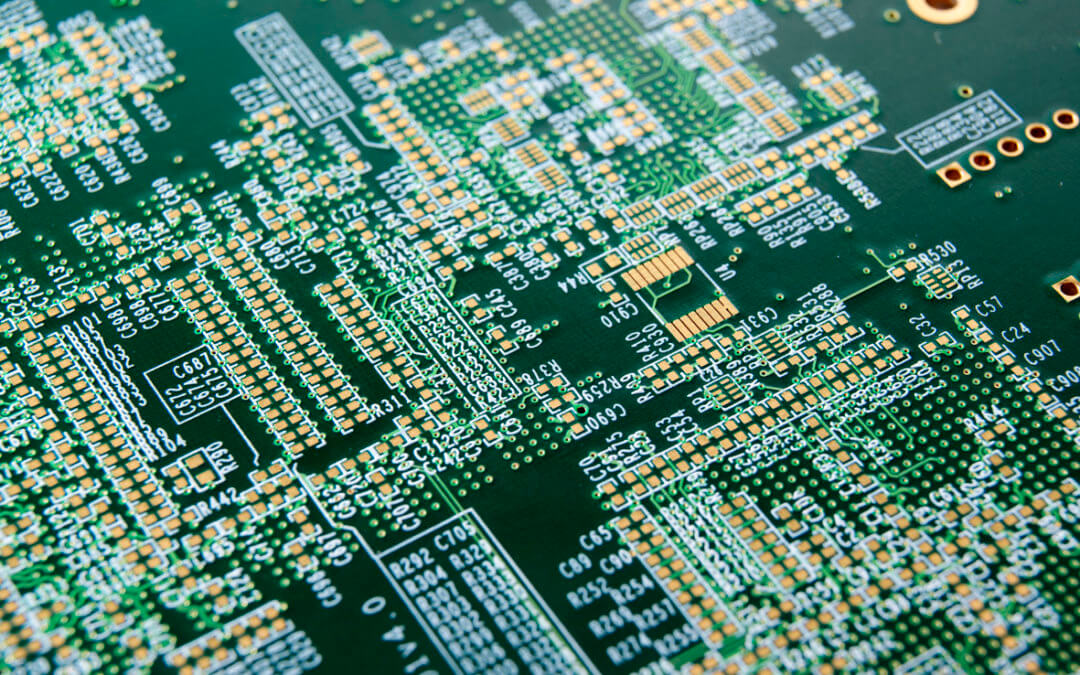
A mid-size OEM might introduce 10 or 20 prototype designs in a year, or even fewer, whereas an EMS partner, set up to deliver volume and efficiency, will produce several hundred in the same time period. When EMS providers engage with customers early in the design process, they can apply their combined years of industry expertise and innovation to ensure the end result is as effective and efficient as possible. For example, we have accomplished engineering staff aligned to all aspects of design from pure PCB design and assembly to mechatronics, software engineering, COTS (commercial off-the-shelf) module integration, interface design, electrical design, enclosures, prototyping, testing and certifications or any task that brings life to a product.

Align component selection to Design for Manufacturing (DfM) principles

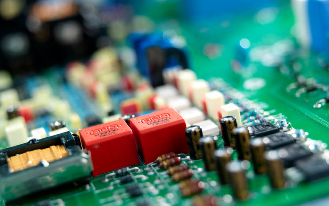
A customer may present us with schematics for a product design that aren’t feasible or could be improved. A problem we increasingly encounter is when hard-to-source MLCCs (Multi-Layer Ceramic Capacitors) are specified instead of more readily available polymer alternatives. It could be they’ve designed-in an EOL (End of Life) component or they’re proposing a needlessly complex PCB layout.

Early engagement allows for product optimisation using DfM principles. This is the practice of designing products with the manufacturing process in mind, choosing the best processes, materials and components. For example, we look at ways to minimise the use of new ‘active parts’ in favour of standardised, widely available components, as the design of a new part is usually only the best option from a purely inventive design point of view. DfM addresses this by asking designers to consider not what could be created, but what should be created. Minimising active parts through standardisation simplifies product design and leads to operational efficiencies through lower inventories.

DfM is not about discouraging creativity and new solutions; sometimes it is necessary to develop a new part. However, this approach ensures manufacturing costs stay low without cutting corners and the best results are achieved without compromising on quality or performance.

Help with front-loading the manufacturing process

Once a design is released to production, and especially after it has been validated for regulatory compliance, the costs of changing the design may be prohibitive. In fact, decisions made during the design phase determine 70% of the product’s final cost. There is often a singular, and closing, window of DfM opportunity that must be grasped to avoid later complications. Working closely with contract manufacturers while designs are still fluid ensures that both manufacturing and supply chain considerations are factored into your manufacturing plans.

By front-loading the process, an early review of all the commercial aspects of the design can be conducted, including but not limited to:

  • Design resilience and compliance aspects
  • Product and process design that balances product quality against design effort
  • The effort involved to design new active parts and costs of inventories
  • Use of alternatives for volume-friendly production
  • Use of standard parts, COTS modules, etc
  • Global sourcing and associated obsolescence issues
  • Selection of “machine friendly” packaging formats

Let’s take a look at some of these in more detail.

Designing to save cost on material spend

Component cost is a significant factor of DfM. Material spend makes a big difference to OEM profit, especially during uncertain times of fluctuating supply and currencies. By consolidating OEM material spending, an EMS provider will gain a 10-100 fold increase in spending power, providing direct access to global manufacturing channels and cutting out the proverbial ‘middle man’. This is how we can overcome minimum order quantity (MOQ) restrictions and access the very best price breaks. Also, a larger EMS material spending power means that components can be sourced in machine-friendly formats which increase automation and traceability, further enhancing product integrity and overall performance.

Factoring-in supply-chain considerations

Component availability and obsolescence issues are increasingly a problem for product design. We are well positioned to help a customer navigate through these issues. Even the most perfectly designed electronics assembly, presenting zero fabrication, regulatory or inspection issues can create critical delays and costly substitutions if components are not sustainably available.

These supply chain breaks may be due to:

  • Changes in distribution
  • Components being placed on EOL
  • Stocks being allocated as they run low
  • Or mergers and acquisitions creating ever-widening ripples

Product design engineers are often focused on component selection to achieve the desired functional performance and sometimes struggle to see beyond the immediate prototype or small-batch production stages.

We provide valuable input to help create selections that are sustainable and cost-effective, addressing future requirements when the product ramps into eventual production volumes or off-shore manufacturing locations.

The challenges facing unmanned vehicle design

Unmanned vehicles are in the news again

Just before Christmas 2018, hundreds of flights were cancelled at Gatwick Airport following reports of an unmanned aerial vehicle (UAV) – or drones as they are better known – being repeatedly sighted near the runway.

For three days there were 140,000 passengers and over 1,000 flights affected but, despite strong police and military involvement, no credible suspects are yet to be identified.

Unmanned vehicles in themselves are nothing new

Even if we just consider UAVs – as opposed to unmanned sea vehicles (USVs) or unmanned ground vehicles (UGVs) – history tells us that unmanned vehicles (UVs) are not a recent invention.

Nearly 170 years ago the earliest recorded UAV flight was when the Austrian military attacked Venice using unmanned balloons with baskets stuffed with explosives.

UVs remained the preserve of the military for many years. By 1916 the US created the first pilotless aircraft for use in World War One and it was rolling out the first remote-controlled during World War Two.

Until the 80s drones were still largely considered an unreliable and expensive toy, but Israel’s UAV-led victory over Syria in 1982 changed this.

UVs are the disruptive tech par excellence

UVs are set to transform our society – our military capabilities, our industrial operations, our commercial services and our daily life.

It still remains true that today many of the most notable drone flights have been conducted for military purposes.

But not for long.

Goldman Sachs predicts that by 2020, 30% of what is estimated to be a $100 billion global UAV market will be consumer or commercial rather than military.

Already drones are widely used for agriculture, aerial photography, geodesy, law enforcement, advertising and building safety.

In the near future UAV taxis may be on the cards, Amazon has been publicly investigating UAV deliveries since 2014 and drones may emit radio/video signals – or other forms of bandwidth – for connectivity in rural areas.

Meanwhile, under the ocean and across the roughest of terrains…

UV potential is already widely used by oceanographers and the oil and gas industries to carry out work in depths that would create a host of problems for manned sea vehicles. In the surf zone and on land, UGVs are used to scan and neutralise mines. Across difficult terrain, they are reducing operational demand for troops travelling cross-country and in commercial plants, they are used for surveillance.

In fact, UVs in general tend to be used to accomplish the 3 ‘D’s – work that is too dull (or repetitive), dirty or dangerous for humans to carry out.

And herein lies one of the biggest challenges for OEMs when they begin to design UVs.

The design challenge of UVs

An experienced, quality EMS partner will reduce manufacturing risk, increase operational efficiencies and overcome technical challenges for OEMs entering the UV market.

Typically, UVs are put to use in hazardous – or at least challenging environments.

  • UGVs must withstand the knocks and bumps of rugged terrain
  • USVs often operate in deep sea environments and must withstand intense atmospheric pressure and the corrosive force of salt water
  • Surf zone mine sweepers face the risk of explosions and the pounding force of the ocean as they prepare the way for troops

To design UVs that can withstand such situations an in-depth understanding of suitable casings is essential, as is the ability to pack a lot of functions into a small space.

Many UVs are reliant on as large a battery as possible to deliver sufficient operating times. And the larger the battery the more compact the space for other essential electronics.

Rapid improvements in battery technology mean that the energy density of lithium-ion batteries is improving by 5 to 8 percent every year: their lifespan is expected to double by 2025.

But system integration can unlock equally mission critical doors for UVs as their power sources can.

System integration is vital for designing efficient, effective and robust UVs. It takes a specialist EMS partner to skillfully design and integrate custom PCB assembly with sub-assemblies and modules, enclosure design, fabrication, cabling and wiring.

All these elements are used to create complex, multi-tier systems that marry robotic functionality with vehicular design. And each design is made ready through testing, software, programming and calibration.

Factors such as size and weight are critical here – but so too is longevity, resistance to environmental forces and reliability. Materials must be selected to offer protective enclosures that are able to withstand factors such as immense pressure, intense heat, corrosive forces and jolts, impacts and explosions.

Yet, these rugged exterior and interior casings must protect incredibly complex and intricate electronics that are at the forefront of developments in navigation, control systems, robotics, communication and connectivity.

Where IoT capabilities are employed for security or data collection, it is also vital that the electronics are not only robust enough to handle challenging environments but also offer maximum security and defence against cyber-attacks.

All of these layers of complexity call for a specialist EMS partner – and for one who can confidently prototype for successful and effortless integration into wider systems.

Why choose Chemigraphic as your UV EMS partner?

Chemigraphic has been supporting complementary market sectors that include the oil and gas industry, aviation, aerospace, military and transport for many years. Our knowledge of and experience in designing, assembling and fulfilling products destined for hostile and challenging environments means we can help you design, prototype, and run rigorous tests to ensure reliability and the best possible results for your UV.

Feature photo by Lance Cpl. Rhita Daniel.

Best practice in managing a product’s end of life

Apple’s announcement in November 2018 that is was to cease the reporting of iPhone sales volumes really worried investors. A flattening of sales, combined with doubts over Apple’s projected innovation, impacted on its stock price. Around the same time, Chinese tech giant, Huawei, beat it into third place on smartphone sales and even set their sights on surpassing the leader, Samsung, with promises of foldable screens and artificial intelligence. Technology pundits began suggesting the unspeakable: the very beginnings of the iPhone’s end of life.

foldable phone

Source: World’s first foldable smartphone unveiled

OEMs can sometimes struggle to manage product end of life effectively. Instead of managing the process from an early stage, they focus all their attention on maintaining sales. History shows that even Apple can be caught off guard.

The iPod – From 1000 songs in your pocket to none

Apple introduced the first-generation iPod in October 2001 with the slogan “1,000 songs in your pocket”. Second, third, fourth and fifth generations followed until September 2007 when Steve Jobs unveiled the 6th Gen iPod “Classic” with a new, thinner chassis and a better battery life. The last hardware update occurred in 2009, and then in September 2014, it was finally discontinued. Apple CEO Tim Cook told us one of the reasons at the 2014 WSJD Live event: “We couldn’t get the parts anymore, not anywhere on Earth”. Even Apple, the first US company to achieve a $1,000,000,000,000 market value is subject to the same pressures as every other large electronics manufacturer.

ipod classic

There are many reasons that a product may enter an EOL process: component shortages, technology barriers, functional redundancy, competitor activity and a lack of investment that causes old or worn tooling can cause and accelerate product decline. It remains a truism that all good things must come to an end; what makes a difference is how you manage it.

Best practices and strategies for managing EOL

Since product decline is inevitable, lifecycle support is an essential service that an EMS partner should provide to its customers. Different solutions can be applied to end-of-life situations: some products get superseded by newer models or versions, meaning only slight tweaks to the manufacturing and sourcing procedures. Other products may simply need support as they dwindle, which can involve investing in enough stock and parts to last the predicted period before obsolescence. Sometimes it’s necessary to re-invest in alternatives. We can advise our customers, ensuring money and resources are not wasted. 

Manage EOL early within a Product Lifecycle Plan

Every product goes through a similar Product Life Cycle (PLC) – introduction into the market, growth, maturity, and then a decline with EOL. Products should, therefore, be managed within a Product Lifecycle Plan, covering all aspects of the product development, from conception to the disposal of the product and components. Start-up manufacturers often overlook this critical aspect but a skilled EMS partner will be able to help develop such a plan.

 Product Life Cycle Curve

Allow products to evolve

Although the iPod was eventually doomed by component shortages and alternative technologies, Apple foresaw the trajectory of the smartphone and rightly predicted how the iPod would become all but redundant. Is that possible with the iPhone too? Ask most tech companies which product is likely to replace the smartphone and the most probable answer will be something “wearable”. The Apple Watch is likely to see many evolutions, as it changes in shape, size, and functionality to communicate with a plethora of smaller IoT devices that are likely to surround us in the future. In an ever-changing global landscape, agile lifecycle support for products is critical. An EMS manufacturing partner can help you make the evolutions from one generation to the next.

Manage component shortages by investing in stock to guarantee a lifespan

As we saw in the iPod example, component shortages can accelerate product decline and in extreme cases force an OEM into sudden and radical design changes. An EMS partner can assist during times of shortage by staying on top of these issues and combining financial leverage to secure large amounts of stock on behalf of clients as well as buffering to provide uninterrupted supply. Chemigraphic operates a demand-based MRP (Material Requirements Planning) system, which ensures on-time delivery, material presentation requirements, stock accuracy and component batch traceability.

Change management

New regulatory requirements, responses to field performance issues and specification adjustments can all drive the need for design and process changes. Following the introduction of RoHS compliance, for instance, many components became unavailable available, due either to the rationalisation of component manufacturers’ production lines, or to have had their part numbers changed. To assist our customers – many of whom are exempt but have stringent approval criteria to meet – we have introduced a fully comprehensive process to verify that the RoHS approved alternative is acceptable before offering it to our customer for their approval. An experienced EMS partner provides flexible and responsive change management to ensure cut-in is effective, controlled and pain-free.

Don’t overlook the value of returns, repairs, and warranty.

Customers may choose their EMS partner to manage aspects of their returns procedures, typically for in- and out-of-warranty support, root cause analysis; or to repair/refurb products to sell as used. Revenue can be gained through these channels that may influence a decision to maintain or discontinue a product. Chemigraphic frequently takes on aspects of this process, since we have access to the components as well as testing experience to rectify product faults, plus the automation and logistics skill to make this process as efficient as possible.

Communicate clearly to customers

Customers will be more critical of businesses that cannot smoothly manage the transition from older products to new versions. Some customers will not upgrade, so it remains particularly important to clearly communicate when and what is being eliminated and help them find a solution.

From art to science – the development of the PCB

From-art-to-science-1080x675

We recently outlined the evolution of the PCB after it emerged to replace point to point connections on a chassis in the years following World War II.

Here we’d like to trace the key moments in recent years that our brief history did not allow us space for.

As we chart how the manufacture of PCBs transformed from an art to a highly-specialised science we pinpoint five decisive moments that have kick-started their development in recent decades.

In the beginning

The earliest PCBs were very much works of art.

Etched by hand, they owed more to technology from artwork reproduction than to high tech.

To create these circuits copper-clad boards were used. The artwork was hand-drawn, and once the track layout was defined, it was printed onto the board as an etch-resist mask. Acid was next used to etch away the exposed copper before another chemical removed the etch resist.

Although we would still recognise the circuit board produced today, the process of producing it had its roots squarely in methods that had long been used in printing and artwork reproduction.

These processes have changed much since the tech breakthroughs and the manufacturing and electronic development that came to a head in the 1990s.

Here are just five of the ways that PCB manufacture was transformed from an art to a science.

The multilayer breakthrough thanks to via

It was in the 1990s that the use of multilayer surface boards became more frequent, allowing for greater complexity and speed.

The inevitable reduction in size of PCBs allowed them to be incorporated into a wider range of designs and devices.

What  the introduction of blind via and buried via permitted was connection on different layers through copper-plated holes functioning as an electrical tunnel through the insulating substrate. In the past connection through layers had been allowed using plated thru-barrels, but these created an obstacle to connections to every other layer.

The result, following the introduction of via technology in 1995, was the production of High-Density Interconnect (HDI) PCBs.

These could accommodate a much denser design on the PCB and allowed the use of significantly smaller components. With multilayer HDI PCBs reliability is enhanced in all conditions, which is why the most common applications for HDI technology are computer, mobile phone components, medical equipment and military communication devices.

Via have continued to evolve, with the recent emergence of micro-via, a specific type of small via which is used on particularly high-layer-count, densely populated PCBs, which are typically performing some form of high-speed number crunching.

Leadless components and the shrinking PCB

As we’ve seen PCBs really started to shrink in the 1990s (and they haven’t stopped since). Alongside the use of micro-vias we also saw the advent of leadless component designs, such as BGAs, uBGAs, chip-scale packages and so on.

These paved the way for integrated circuits with more gates which ushered in the start of successfully embedding memories and Systems on Chip (SoC) together.

Leadless packages save space by keeping the contact points in a matrix underneath the component instead of squeezed side-by-side around their perimeter. This extra space is crucial for applications like mobile devices, tablets and wearables, where every millimetre counts.

However, leadless packages also have a great deal of mechanical strength, so they don’t separate from PCBs as easily. This is thanks to their high contact area to package ratio which allows them to withstand a great deal of pulling and shear forces.

Since leadless devices are suspended on a matrix of underside solder spheres rather that soldered pins around the perimeter, manufacturing and inspection techniques need to be much more sophisticated, but the space-efficiency and reliability benefits are compelling.

Flexible circuits transform PCB designs

It was, again, in the 1990s that flexible circuits really made their presence felt, although their history can be traced all the way back to the birth of the PCB itself.

With the first PCB manufactured by Paul Eisler less than a decade old, we find a published exploration by Cledo Brunetti and Roger W. Curtis in 1947 of creating circuits on flexible insulating materials. Indeed, by the 1950s Victor Dahlgren and Royden Sanders had already made significant advances in actually developing processes that could print and etch flat conductors on flexible base materials.

Today, flexible circuits are produced by mounting electronic devices on flexible plastic substrates (such as polyimide, PEEK or transparent conductive polyester film) or by screen printing silver circuits on polyester.

They offer several advantages for many applications. These include their potential to replace multiple rigid boards, their suitability for dynamic and high-flex applications and their ability to be stacked in various configurations.

You will find them in:

  • Tightly assembled electronic packages, where electrical connections are required in three axes, such as cameras.
  • Electrical connections where the assembly is required to flex, such as folding mobile phones and laptop screen hinges.
  • Connections between sub-assemblies to replace the bulky and heavy wire harness, such as in cars, laptops, rockets and satellites.
  • Electrical connections where board thickness, weight or space constraints are important factors.

The finishes that created new beginnings for the PCB

The range of finishes that have been introduced into PCB manufacture over the last 20 years has also greatly enhanced their suitability for use in a number of applications.

The finish is applied to ensure solderability and to create the base of electronic connection between board and device. But, the correct surface finish selection can also affect PCB reliability – and the introduction of new finishes has greatly enhanced their reliability under a number of different conditions.

  • HASL

The traditional finish is Hot Air Solder Levelling (HASL) but this is now increasingly being replaced by lead-free HASL.

All HASL finishes prevent oxidation from the underlying copper but the process causes high stress on the PCB and this can diminish its long-term reliability. The process is also not suitable for HDI PCBs.

  • ENIG

ENIG (Electroless Nickel Immersion Gold) offers a great alternative – but one that comes with a price tag.

Ideal for fine pitch, flat surfaces, ENIG perfectly suits the modern-day HDI PCB. It can, however, carry undesirable magnetic properties and is prone to a build-up of phosphorous that may cause faulty connections and fractured surfaces.

  • OSP

OSP (Organic Solderability Preservative) is a finish that can be considered for fine pitches, BGA and small components. In addition, it is less expensive than ENIG and highly repairable, but it is difficult to test and has a limited shelf life of six months.

The rise of the exotic substrate

PCB manufacture has over the years gradually settled on the glass epoxy laminate of FR-4 as its preferred material.

There is good reason for this – in terms of performance and affordability – but we have, in recent times, seen the introduction of a number of alternatives. These ceramic and metallic substrates are often suited to specialist applications, such as those requiring performance in conditions of high temperature and high power.

They include:

  • Aluminium
    Used for parts requiring significant cooling, such as power switches and LEDs.
  • Kapton
    A polyimide foil used for flexible printed circuits that is resistant to high temperatures.
  • FR-5
    Woven fiberglass and epoxy offering high strength at higher temperatures.
  • G-10
    Woven glass and epoxy offering high insulation resistance, low moisture absorption and very high bond strength.
  • G-11
    Woven glass and epoxy offering high resistance to solvents as well as high flexural strength retention at high temperatures.
  • RF-35
    Fiberglass-reinforced ceramics-filled PTFE (Teflon) offering good mechanical and high-frequency properties.
  • Polyimide
    A high-temperature polymer offering excellent performance that can be used from cryogenic temperatures to over 260 °C.

The return of the art of the PCB

The diversity of today’s PCB technology requires an artist to create the perfect board for each device, application and customer.

Chemigraphic has the broad expertise and capability in each specialist area to understand and decide which technology and processes will create the right PCB for your requirements and budget.

Is the future of manufacturing additive?

The potential uses for 3D printing were widely misunderstood when it first appeared on the scene.

Tech pundits and futurologists joined forces to proclaim that 3D print would usher in a consumer revolution, as individuals took control of the means of production for themselves.

But, as we highlighted in our last blog, the benefits of 3D printing are now actually reshaping the manufacturing sector, rather than making it redundant.

The trend towards Additive Manufacturing

You can chart the change in the perceived benefits of 3D printing. As it changes from being seen as a consumer tool to a production tool, the use of the term ‘Additive Manufacturing’ (AM) dramatically rises.

This is how searches for AM are reported by Google Trends:

additive manufacturing

3D printing and AM are now used interchangeably as terms.

Peter Zelinski, the editor-in-chief of Additive Manufacturing magazine, reminds us we should bear in mind that AM also refers to other technologies and processes.

These include:

  • Rapid prototyping
  • Direct digital manufacturing
  • Layered manufacturing
  • Additive fabrication

Revealing synonyms

Synonyms, other than 3D printing, that are increasingly used for AM hint strongly at the benefits it offers – and that we will review further below:

  • Desktop manufacturing
    Suggests how AM frees production from the tyranny of tooling
  • Rapid manufacturing 
    Echoes rapid prototyping
    Suggests the speed of both prototyping and manufacture that 3D print offers
  • On-demand manufacturing
    Echoes on-demand printing
    Suggests the ability to cost-effectively create bespoke, tailored products


Additive Manufacturing

AM describes any technology that creates something by cumulatively adding layers of material.

The range of materials that can be used is ever-expanding and includes plastics, metals and concrete. In the very near future advances in biotechnology will inevitably see human tissue included in this list.

The basis of AM is computerised 3D modelling (or CAD). The data from this is used to add successive layers of liquid, powder or sheet material to manufacture a 3D object.

AM is fundamentally different to traditional manufacturing processes. These typically have a high up-front cost that is related to the need to create tooling.

  • Moulds are required by formative manufacturing technologies (such as injection moulding)
  • Cutting tools are needed for subtractive technologies (such as CNC machining).

The uses of Additive Manufacturing

This is what AM does well:

  • It is best suited to the production of single (or a limited number) of parts
  • It has an incredibly quick turnaround time
  • It has very low set-up costs
  • It can produce complex geometric shapes that are not producible using traditional manufacturing methods

In the past it was the case that the lower strength of objects it created could be an issue – and similarly it had proved wanting where functional parts with tight tolerances were called for – but this is increasingly not the case.

For instance in 2017, Siemens created the first gas turbine blades ever produced using 3D printing. Following performance testing under full-load conditions, these blades were found to survive temperatures above 1,250oC and pressures similar to the weight of a double-decker bus.

 Siemens created the first gas turbine blades ever produced using 3D printing

Source: Future Makers

What’s more, the blades traditionally took over a year to make but, with 3D technology, they took just eight weeks.

Early uses of AM harnessed its benefits for rapid prototyping, but more recently it is being used to fabricate end-use products in aircraft, dental restorations, medical implants, automobiles and even fashion products.

“This technology will impact pretty much every market sector, whether it’s shoes, whether its clothes, automobile parts, aeroplane parts, medical devices or electronics.”

Michael Todd, Global Head of Innovation at Henkel

Source: 3D metal work printing (image courtesy of Davidfotografie/Arup).

The benefits of Additive Manufacturing


The speed of production and lack of tooling requirements are a big plus for manufacturers. They enable designers to rapidly and cost-effectively prototype designs for verification and testing. In the past it took days or even weeks to receive a prototype – now AM places a model in the designer’s hands within hours.

This speed is further enhanced by the efficiencies AM can offer. Most parts require a large number of manufacturing steps to be produced traditionally, but AM completes the build in just one step. Freed from the constraints of, for example, machining and welding, new designs and possibilities can be explored.

For single (or low) volume runs, AM’s lack of tooling offers distinct cost advantages. It removes the need for a skilled machine operator to be present during the manufacture.

It is these cost and time benefits that have led to many innovative uses of AM. Nowhere is this more so than in the production of customised products. It is now possible to reduce the cost of bespoke products such as dental implants, hearing aids, prosthetics and, perhaps even in the near future, body tissue.

As well as medical and dental uses this capability is also seeing AM used for specialised military, automotive and aeronautical parts, as well as for customised fits on sporting equipment and fashionwear.

Is additive manufacturing the future?

As consumer trends move toward customisation, and increased competition demands lower and lower lead times, there is a clear place for AM in the future.

And it’s looking like it can disrupt niche manufacturers requiring specialist tolerances and precision as well as those serving the mass, consumer market.

At present, there are two main factors that restrict its use:

  • Scalability
    AM still can’t cost-effectively manufacture higher volumes of products
  • Versatility
    The range of materials that AM can use for manufacture is expanding but, for example, it still struggles to handle true silicones

However, its capabilities are continually expanding.

And it’s here to stay.

Richard Hague, Professor of Innovative Manufacturing at the University of Nottingham, firmly stakes its place in the future of manufacturing:

“I don’t think additive manufacturing is an emerging technology any more. I think it’s emerged, and many people are already using it – and using it successfully.”

How is 3D printing freeing up design space?

“If by some miracle some prophet could describe the future exactly as it was
going to take place, his predictions would sound so absurd, so far-fetched that everyone would laugh him to scorn.”
Arthur C. Clarke, author, speaking in 1964

Science fiction writer Arthur C. Clarke went on from making this observation to describe the forthcoming advent of 3D printing.

And, sure enough, it came to pass.

Today, as 3D printing quite literally breaks the design and manufacturing mould across a range of sectors, it’s time to assess its true impact and where it may take us next.

The path that 3D printing has taken bears very little resemblance to what the prophets foresaw. Throughout the early years of the new millennium, futurists prophesised it would usher in a new consumer society. In this brave new world, the need to visit shops to buy things would be gone – and so too would the need to rely on online retailers’ massive warehouses to deliver our goods.

Soon, we were told, we would all be downloading a design file to our personal 3D printer and manufacturing our products – exactly as we wanted them to be – from the comfort of our homes.

Of course, this consumer revolution never happened.

However, a sea-change is quietly washing over the design, manufacturing and production sectors, one that is not deluded tech fantasy, but very real indeed.

Richard Hague, professor of innovative manufacturing at the University of Nottingham, compares the hype and reality of 3D printing with the dotcom crash of the late 90s.

“There were all these expectations about what the internet would do, and then the hype disappeared. But meanwhile, in the background, people were forging ahead, and actually some major industries emerged after that point. I think that’s where we are now.”

We’re going to look in more detail in our next blog at how 3D printing has led to additive manufacturing. We’ll chart how its disruptive potential is transforming the processes used – and products made – by sectors as diverse as medical, military, automotive, aerospace and electronics.

First, though, in this blog we’re going to highlight how 3D printing has also been freeing up the design space in which new products can be imagined and then tested.

3D printing and design

Let’s start with the basics.

There are a number of ways to print in 3D, but all are based on creating a digital model as a physical three-dimensional object by the gradual addition of material a layer at a time.

It is this process of addition that makes 3D printing a radically different way of manufacturing. Traditional technologies are based on subtraction from materials (such as CNC machining) or forming these existing materials (such as injection moulding).

One of the key benefits of 3D printing is that no special tooling or moulds are required – and this leads to many of the benefits we discuss below and in our next blog.

The 3D printing process is initiated directly from the digital model that forms the blueprint of the manufactured object. This model is sliced by the printer’s software into incredibly thin, 2-D layers and these are translated into the machine language (G-code) that the printer executes.

It is at this stage that 3D printers differ in their operation. For example, desktop FDM printers melt plastic filaments that are laid down through a nozzle, whereas large industrial SLS machines use lasers to melt (or sinter) thin layers of metal or plastic powders.

For more information about 3D printing technologies, this excellent guide from 3D Hubs details the differences.

Despite the possible production speeds of as little as four hours, it’s important to note that 3D printed parts often require some post-processing (usually manual) to achieve the desired level of finish.

3D printing and design benefits

Generally speaking, 3D printing is the best option when:

  • A single (or only a few) parts are required
  • A quick turnaround time and a low-cost is needed
  • When the part geometry cannot be produced with any other manufacturing technology
  • When high material requirements and tight tolerances for functional parts are not essential

Faster verification of designs

One of the main advantages of 3D printing is undoubtedly the speed at which parts can be produced compared to traditional manufacturing methods. The lead time on an injection moulding die alone can be a finger-tapping matter of weeks.

Complex designs can be uploaded from a CAD model and printed in a matter of hours. This offers designers rapid verification of design ideas.

It cuts out the need to create tools to create parts and also places the capabilities of production within the working space of the designer themselves – as opposed to at a plant that may be geographically remote from them.

Efficiencies

3D printing allows designers to manufacture products and parts as efficiently as possible, cutting down on the number of manufacturing steps required by traditional technologies. These may include cutting, welding, polishing, drilling, mounting, sandblasting, priming and painting. 3D printing can complete all these steps as one, with no interaction from the machine operator.

Cost-savings for prototypes

Particularly where labour costs are concerned, 3D printing can slash the design costs for manufacturing prototypes.

Post-processing aside, the majority of 3D printers only require an operator to press a button. Compared to traditional manufacturing’s reliance on highly skilled machinists, the labour costs for a 3D printer barely register.

This means that for the creation of prototypes that verify the form and fit of a product, 3D printing is significantly cheaper than other methods.

Freeing up design space

The restrictions of traditional manufacturing on what can and can’t be made hold much less relevance for 3D printing. Design requirements such as draft angles, undercuts and tool access do not apply to designers using additive manufacture.

This gives designers a large amount of design freedom and enables the creation of very complex geometries.

Customisation

Another freedom that 3D printing allows is the ability to completely customise designs. As additive manufacturing technologies excel in building single parts one at a time, they are perfectly suited for one-off production of unique, bespoke designs.

Source: Wired 

This ability has transformed the medical and dental industry to realise the manufacture of custom prosthetics, implants and dental aids. High-level sporting gear can now be tailored to fit an athlete perfectly and the fashion industry is also proving quick to realise the custom design benefits of 3D printing.

Source: 3D natives

The brave new world of 3D printing

We opened with a quote from Arthur C. Clarke suggesting that prophets of the future risk appearing ‘so far-fetched that everyone laughs them to scorn’.

The design benefits of 3D printing are not far-fetched hype: they are here, they are happening and they are making a real difference to the world we live in.

In our next blog we’ll look at how these benefits are not only transforming design but manufacture itself.