Trump’s tariffs will come back to haunt him

Chris

Trump’s tariffs will come back to haunt him: The US will end up as the isolated party if it ignores the scope of China’s trading potential

Chris Wootton, CEO, Chemigraphic

“As the trade war between the US and China ramps up and President Trump continues to threaten to impose tariffs on imported products from China, businesses across all industries are naturally starting to feel nervous about the implications of such a move. Tariffs will no doubt lead to a multitude of complications across import, manufacturing and retail sectors and the effects will be felt by many.”

“The latest development in the tariff debate has seen China attempt to calm the waters by offering to buy US goods to the tune of $70 billion over the next year if the tariffs are called off, so a resolution may be on the horizon. It seems inevitable that at some point, Trump will have to back down and come back to the table to discuss the issue further, even if it’s not immediately.”

“If the Chinese tariffs are imposed, costs of goods in the USA will increase and, although the consequences won’t be apparent immediately, within 12-18 months, the landscape will change, consumers will start to see the prices rise and there will be unrest and backlash.”

“The fact remains that no country is self-sufficient and the isolation of any nation, whether physical or in terms of trade, is a dangerous proposition. China itself is too large and too successful to be isolated; it makes too much and we buy too much of it for it to be effectively cut off. Even if the US administration does go ahead with its plans, other nations will no doubt take advantage of the low costs, better pricing and widespread manufacturing capabilities that China offers. This in turn will drive the success and popularity of other low-cost regions, and effectively, the US itself will become the isolated nation as countries start to shift their focus elsewhere.”

“As an EMS, the benefits that China offers in terms of manufacturing and sourcing electronic components are too extensive to ignore. We opened our new sourcing office in Shenzhen in January and already, our customers are benefitting from the higher volumes and lower costs  of component parts thanks to the access to China’s pricing structures we can now offer.”

“With regards to the future, I’m sure the situation will produce some fireworks for some time to come, as political tensions rumble on and industry faces the consequences of decisions made by the US leadership. But I’m also confident that it will normalise and calm down over time. Probably via a change in that very leadership….”

Manufacturing electronic products for harsh and hazardous environments

Manufacturing electronic products for harsh and hazardous environments

John Johnson, NPI Director, Chemigraphic

A number of our customers develop and operate products in highly hazardous environments, from sub-sea conditions to explosive atmospheres and areas contaminated by harmful chemicals and substances. These products have to be robust, protected from outdoor or harmful elements and technically sound in order to deliver excellent functionality and performance in these conditions.

Inevitably, this requirement adds a layer of complexity to the manufacturing process and in particular, EMS activity. At Chemigraphic, we work extensively with companies developing and operating products in hostile conditions and always adhere to the following practices when dealing with these environments.

1. Check parts are correct to specification

Products which are designed for use in high risk areas, such as those which are contaminated with toxic substances or carbon dust, have to be manufactured in a way that ensures they can withstand contact with these particles.

The first consideration with these products is to ensure that all “critical parts” are correct to specification, via thorough inwards inspection criteria and ongoing quality checks and testing. For example, faulty or poorly specified circuitry could in theory lead to an over-current fault condition, which could then overheat and cause a fire and then an explosion. This means it is critical to vet and validate each supplier robustly, meaning sources are reputable and batch traceability is ensured.

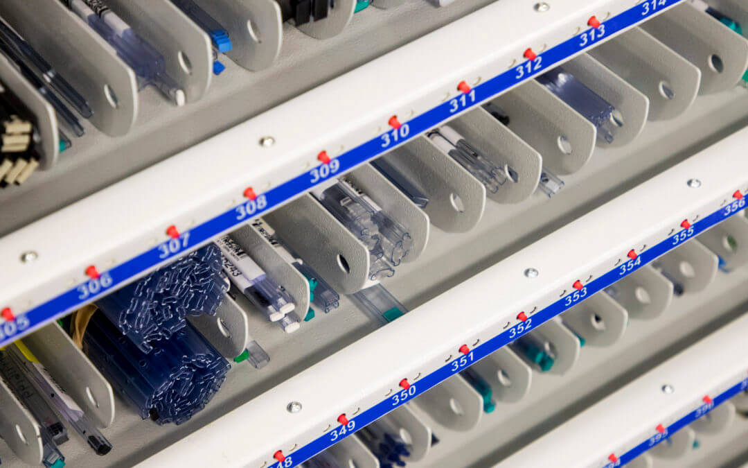
We then employ systems with sufficient material control governance to ensure that only the correct parts are fitted into the right locations. This can be challenging when the vast majority of small footprint SMT components do not have markings and are visually identical. In addition, the volumes in consideration are vast: a kit of parts for a sophisticated PCB might run to 500-600 distinct lines. Part of the solution is to optimise the use of barcoding and intelligent materials trace, such as RFID enabling and JUKI-automated kitting, a process exclusive to Chemigraphic in the UK. As with a large proportion of our operations at Chemigraphic, we use smart, data-driven automated processes which can be controlled and measured without the risk of human error or inconsistencies.

2. Protect products using specialised techniques

There are a number of circumstances which require electronic products to function and perform in extremely challenging conditions, for example sub-sea environments. Products used in these areas include those in oil and gas research facilities, marine industry operations and sub-sea rovers or maintenance machinery.

Manufacturing products for underwater environments comes with a variety of serious challenges, such as erosion caused by salt and force of the water. Salt in particular is extremely corrosive and can literally eat through metal components and casings. In these cases, we apply specialist conformal coatings and sacrificial layers to product structures and internal circuitry, protecting them from salt and other corrosive substances.

We apply these coatings with robotic, automated processes to increase cost-effectiveness and consistency. Encapsulation of circuitry provides an extra level of protection for the components, effectively closing them off from external elements.

Microscope harsh and hazardous environments

3. Apply additional engineering processes

In circumstances involving explosive atmospheres and flight conditions, such as those in defence and transport industries, extra measures need to be taken to ensure products are robust enough to survive take off.  This particularly applies to devices with motion potential such as gyroscopes, valves and actuators. In these conditions, ensuring products reach Intrinsically Safe (IS) standards is vital, and something we are highly skilled and experienced in at Chemigraphic.

In these conditions, it’s vital to ensure optimal assembly integrity starting from bare PCB rigidity, where thickness and copper weight need to be balanced against payload constraints. Due to the extreme temperatures and hostile environments involved, solder integrity also becomes critical and the base process needs to be robust and repeatable.

4. Data analysis and smart manufacturing

 With any manufacturing process, it’s essential to keep comprehensive records of activity and processes. However, this element is particularly critical when it comes to developing products for harsh and hazardous environments. As so many complex conditions and procedures are involved, it’s essential that every step is prepared, researched and accounted for, with documentation and certification available and presented to customers at every opportunity.

This includes ensuring products reach IS criteria, meet specialist handling requirements and any essential transport requirements, for example with lithium batteries. This allows for continuous control and traceable processes which create evidence of compliance to industry standards and regulatory requirements. Our sophisticated data network at Chemigraphic allows us to monitor and track activity and processes and use this data to implement smart and improved efficiencies throughout our operations.
Q&A with Graham Hill, Facilities Manager

Graham-Hill

Q&A: Graham Hill, Facilities Manager

  1. How long have you worked in this industry?

I began my career in 1976 as a 16 year old apprentice with the Mullard Radio Valve Company in Mitcham, Surrey.  Mullard was later taken over by Philips.  Following the successful completion of the four year Philips apprenticeship, I got a job in the factory as a quality and repair technician in the Electronics Assembly Department. After around five years, I changed direction slightly and joined the Central Materials Laboratory running the photography department. Photolithography was how Printed Circuits were produced before the CAD systems we use today were available.  Philips closed this factory in the late 1980s and I continued working with PCB design at PT Barkley and company in Coulsdon.  Wanting to get back to a more manufacturing based job I had the opportunity to join Chemigraphic in 1994 as a production engineer and the rest, as they say, is history.

  1. Why did you choose to work in this field?

I was never going to be a great academic, was not interested in performing arts and wasn’t particularly sporty, so it was always going to be some sort of practical occupation for me. I considered farming, civil engineering and building trades but in the 1970s hobby electronics was all the rage and I had the opportunity to build my own hifi amplifier whilst still at school. Having loved this project, I decided that a job involving electronics was the way to go.  The part of the process that appealed to me most was putting things together, which explains my fondness for manufacturing. The best days are always the ones where at the end you can stand back and say “I made that today”

  1. What do you love about your job?

The variety. My role at Chemigraphic is very diverse and wide-reaching, and I can honestly say that I can never tell what the day is going throw at me until it starts.  Part of what I do is to define what others are going to be making, be it via technical drawings or via written instruction.  Then there is the face to face part of the job, involving helping our teams assemble things in the best possible way either directly, by observing difficulties or helping them develop techniques to overcome these issues.

  1. Describe a ‘typical day’ for you

A typical day will be spent at Crawley ensuring that as another month draws to a close, targets are met, all systems are working, all customers are satisfied, and all staff are comfortable in their roles. Not an easy task, but one I enjoy pursuing!

  1. What have been the proudest moments in your career so far?

The successful completion of any project is always something to be proud of. Obtaining the final sign-off from building control for the Mezzanine floor that houses our SMD, PCB and Test departments was certainly one of my proudest moments. This required managing third parties including the local authority to confirm that all regulations regarding fire control, lighting levels, air handling and emergency access were all correct and met legal requirements.

A new project which is just starting now is our Apprenticeship training scheme.  Getting this up and running and seeing younger people successfully complete the scheme and secure good technical jobs will be a very big achievement and one I look forward to.

  1. What’s the biggest change or development you’ve seen since working in the industry?

It has to be the digitalisation of almost every aspect of what we do.  In 1976, when I started my career, companies produced PCB assemblies which were every bit as intricate as we do today but just using very different techniques and without a single computer of any sort.  All the way from the board blank layout which was done by line film and photographic techniques to the assembly which was completely carried out by hand.  There were no word processors, no spreadsheets, and no e-mail: things still got done but just in different ways.

Chemigraphic takes steps to mitigate market slowdown in passive component delivery

Components

Chemigraphic takes steps to mitigate market slowdown in passive component delivery

Chemigraphic, the global design-led EMS provider, is working closely with its supplier network and customers to combat an industry-wide delay on the manufacture and delivery of passive electronic components. Lead times for MLCC SMD Capacitors and SMD Resistors have been experiencing extended lead times or allocation times for the last few quarters, and in some cases lead times are now exceeding 50 weeks.

Through continuous market monitoring and analysis, Chemigraphic has been able to stay on top of this issue and secure large amounts of stock on behalf of its customers to provide sustainable supply. However, the market has tightened further over the last few weeks with many manufacturers of these parts no longer taking additional orders. The uptake in demand is also having a negative effect on pricing, with some prices increasing beyond 75%.

In order to maintain supply levels and keep to product delivery timeframes, Chemigraphic is talking directly to its customers to ask that orders are placed as early as possible to ensure the best possible outcomes and avoid delays and interruptions to the supply chain.

John Johnston, NPI Director at Chemigraphic, comments: “Having once been easily accessible, staple electronic components, these parts have seen a huge increase in demand due to growing markets such as smartphones and electric vehicles. As a result, other industry sectors are seeing a huge squeeze on the availability and delivery times surrounding these components, as well as adverse pricing trends.

“We always ensure we regularly monitor the market to stay on top of such trends, and this has enabled us to increase our stock holding of these parts as this issue develops. However, as our analysis indicates these conditions are unlikely to ease for at least the next 12 months, we are asking our customers to work with us to stay on top of demand and allow us to forward plan as far in advance as possible.”

The above news story has also been featured in the following trade publications:

 Design Solutions

 eeNews Europe

 Electronic Specifier

For more information on this subject, read Jemma’s blog on five steps to efficient EMS sourcing.

Chemigraphic’s guide to new developments in PCB technology

What’s new on the board: Chemigraphic’s guide to new developments in PCB technology

John Johnston, NPI Director

As consumer demand for lighter, faster and smarter electronic products continues to increase, manufacturers and their supply chains must develop tighter and quicker processes to meet demand and still maintain quality standards. With lead times being squeezed as a consequence, NPI engineers are challenged with establishing watertight controls and processes in order to deliver products which can be both high quality and fast to market.

For EMS providers, working with PCB manufacturers to develop boards for these products has become an essential part of the development process. As well as sourcing components and materials to meet shorter timeframes, expert engineering is also vital to cope with special and thermal complexities.

This said, it’s also a very exciting time to be involved in PCB development. The growing demand of OEMs and consumers for products to live up to the standards of today’s hyper-connected world has given birth to a number of advancements in PCB technology:

Modular Interconnect Devices (MID)

MIDs are ideal for tiny lightweight devices such as hearing aids, pacemakers or medical implants.

Key features

  • These devices carry electrical/electronic functionality through product housing
  • MIDs are modular, increasing efficiency and reducing assembly times
  • They have more space for additional functionality
  • MIDs are smaller, easy to implant and aesthetically discreet

Microfluidics, Lab on a Chip (LOC)

LOCs are millimetre sized PCBs that integrate a number of laboratory functions. They are developed as a result of PCB laser/plasma micro-via ablation and silk-screen technology, and make OEM consumer products safer to use and cheaper to buy.

Key features:

  • Liquid carrying channels and electrical dams/switches are encapsulated within the PCB
  • Miniaturising chemical reactions amplifies results in order to aid more accurate analysis
  • Consumers are able to conduct medical and pharmaceutical monitoring testing at home

Planar PCBs, the next generation of PCB manufacture

The ‘Planar’ process produces glass flat PCBs (no copper track topography whatsoever), also without micro-feature constraints (track-and-gap). In addition the technology produces solid copper vias increasing PCB thermal robustness.

The majority of challenges faced by EMS providers today are around component placement, especially with the development of Surface Mount and Ball Grid Array components (BGA), and PCB flatness and topography. With Planar PCBs, which were originally developed by photocopier manufacturers to make print-head components smaller and more thermally efficient, these challenges do not apply.

Key features:

  • Planar devices look like conventional PCBs
  • The process of producing Planar PCBs using standalone automation is currently under development by a UK consortium, and is likely to be sold under licence to PCB producers

Growing organic biological circuits and components

This technology is at the cutting edge of electronics development, and will be used for medical implant, AI and supercomputing:

Key features

  • These are organic semiconductors that grow in ordered structures
  • Biological circuits are being developed by companies such as Philips Research
  • The benefits to mankind are without question

A longer version of this article was published in Components In Electronics (CIE) magazine: read the online story here.

Early design engagement with EMS providers is crucial in product development

John_factory

Early design engagement with EMS providers is crucial in product development

John Johnston, NPI Director

For years, OEMs across all sectors have traditionally used huge networks of suppliers, all specialising in different areas and working to varying timescales. Now, driven by rapidly developing technology and increasingly demanding consumers, these businesses are being forced to change their supply chain strategies. In turn, they are putting pressure on their suppliers and partners to design and develop products in ever-decreasing timescales, delivering both quality and cost-efficiency.

EMS partners which manufacture customer’s electronic products on a subcontract basis are often presented with a fully-developed and fixed “Design Package” which defines every aspect of the build. Once supply chains are created and commitment is made to EMS processes, material stocks and supplier tooling (which can be expensive in the case of moulded enclosures and specialist metalwork), further significant design changes can be prohibitively complicated and costly.

The most cost-efficient route to market is to establish crucial early engagement between the EMS teams designing and manufacturing the products and the OEMs’ design departments. Getting manufacturing suppliers involved early on in the design process allows them to fully understand the OEM’s business objectives, and apply its own knowledge to positively aid the product development process, identifying and eliminating potential pitfalls and delays.

In electronic manufacturing, a design for manufacture (DfM) approach is essential, as complex components and processes must be handled with skill, to ensure products are both efficient and profitable. In certain sectors, such as defencesecurity or power for example, additional pressures exist such as hazardous or hostile environments or the need to protect national security. For medical equipment, many of the products created have life-critical uses and so it’s vitally important that they are thoroughly tested at the prototyping stage to ensure excellent performance.

By driving early stage engagement to partner customers through the latter design and product development stages, EMS providers can make sure products are created with optimal efficiency in mind. By proposing sensible, practical, and often relatively minor changes to a product, this approach delivers substantial tangible benefits without disrupting or prolonging the design process or cutting corners in terms of efficiency or quality.

To find out more about early engagement in design, read about our newly opened Chemigraphic design centre.

A more detailed version of this article by John can be found on the Design Solutions website